Polycrystalline-ferroelectric-film-based ferroelectric resistive random access memory

A ferro-resistance change and polycrystalline iron technology, applied in the field of information storage, can solve problems such as small switch resistance, insufficient reliability of memory data retention and fatigue resistance, large data fluctuations, etc., to reduce drift and diffusion, reduce Defects and their control difficulty, the effect of inhibiting the diffusion of elements

Active Publication Date: 2014-08-27
XIANGTAN UNIV
View PDF1 Cites 12 Cited by
  • Summary
  • Abstract
  • Description
  • Claims
  • Application Information

AI Technical Summary

Problems solved by technology

[0004] However, there are a large number of grain boundary defects and oxygen defects in the polycrystalline ferroelectric film, and there are interface defects between the polycrystalline ferroelectric film and the electrode layer, and these defects are difficult to control, and the drift and diffusion of defects will cause the data retention of the memory. Insufficient reliability such as anti-fatigue, relatively small switch resistance, and large data fluctuations

Method used


Image

  • Polycrystalline-ferroelectric-film-based ferroelectric resistive random access memory
  • Polycrystalline-ferroelectric-film-based ferroelectric resistive random access memory
  • Polycrystalline-ferroelectric-film-based ferroelectric resistive random access memory

Examples


Embodiment 1

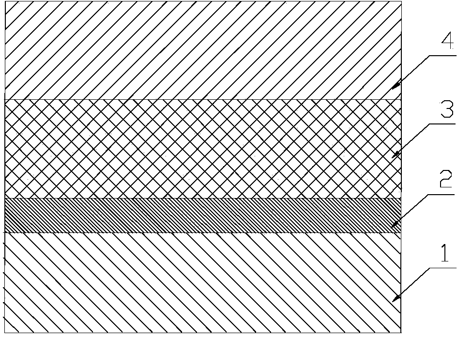
[0033] Preparation of "Pt / (Bi 3.15 Nd 0.85 ) Ti 3 o 12 / HfO 2 / Pt / Ti / SiO 2 / Si substrate" storage unit, the specific preparation process is as follows:

[0034] [1] In growing SiO 2 The single crystal Si substrate (i.e. SiO 2 / Si substrate) to grow the Pt bottom electrode layer. For enhanced Pt bottom electrode and SiO 2 / Si substrate adhesion, under Pt bottom electrode and SiO 2 A 10-20nm Ti adhesion layer is grown between the / Si substrates.

[0035] [2] Growth of HfO on the Pt lower electrode layer2 Defect control layer.

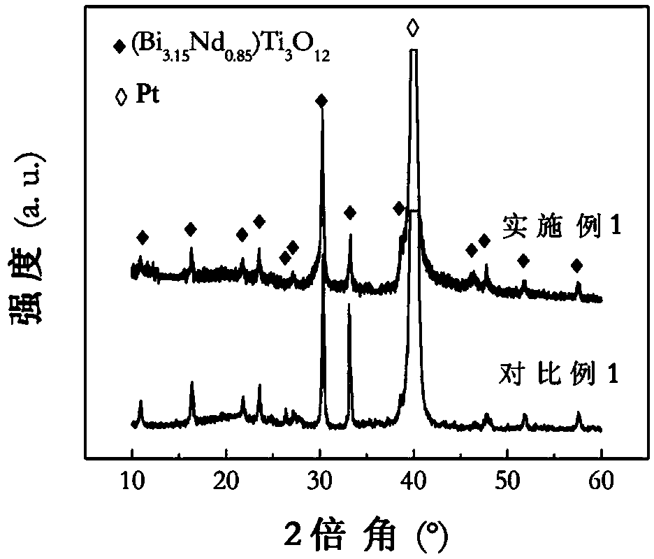
[0036] [3] In HfO 2 Growth on the defect-regulating layer (Bi 3.15 Nd 0.85 ) Ti 3 o 12 Polycrystalline ferroelectric thin film layer.

[0037] [4] in (Bi 3.15 Nd 0.85 ) Ti 3 o 12 A Pt upper electrode layer is grown on the polycrystalline ferroelectric thin film layer.

[0038] The thicknesses of the Pt lower electrode layer 1 and the Pt upper electrode layer 4 are 150 and 100 nm, respectively. The Pt upper electrode is a dot electrod...

Embodiment 2

[0043] In order to illustrate the beneficial effect of the defect control layer between the polycrystalline ferroelectric thin film layer and the upper electrode layer, a "Pt / HfO 2 / (Bi 3.15 Nd 0.85 ) Ti 3 o 12 / Pt / Ti / SiO 2 / Si substrate" memory cell. Except for the HfO 2 layer placed on the Pt upper electrode layer and (Bi 3.15 Nd 0.85 ) Ti 3 o 12 Except for the polycrystalline ferroelectric thin film layer, the others are consistent with the embodiment 1.

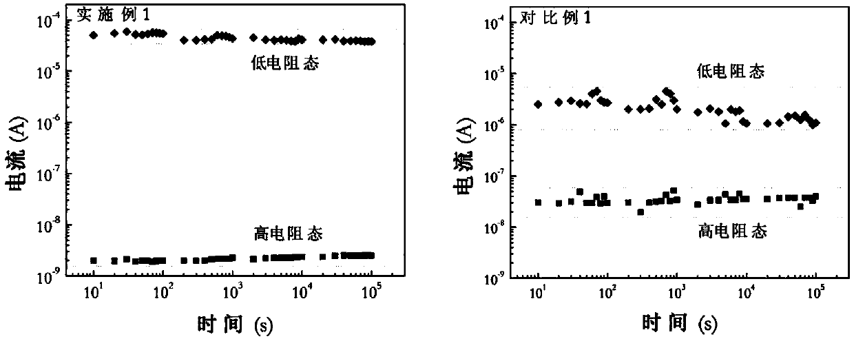
[0044] "Pt / HfO 2 / (Bi 3.15 Nd 0.85 ) Ti 3 o 12 / Pt / Ti / SiO 2 / Si substrate "memory cell memory characteristics similar to embodiment 1, high and low resistance ratio higher than 10 4 ; data hold 10 5 After s, the high and low resistance ratio is still 10 4 left and right; cycle 10 4 After the second time, the high and low resistance ratio is still 10 4 around; the fluctuation of the stored data is small, and the high resistance state current is 9.5×10 -10 ~5.9×10 -9 A, low resistance state current is 1...

Embodiment 3

[0046] In order to illustrate the beneficial effect of having a defect control layer between the lower electrode layer and the polycrystalline ferroelectric thin film layer or between the polycrystalline ferroelectric thin film layer and the upper electrode layer, a "Pt / HfO 2 / (Bi 3.15 Nd 0.85 ) Ti 3 o 12 / HfO 2 / Pt / Ti / SiO 2 / Si substrate "memory cell. Its preparation process except the Pt upper electrode layer and (Bi 3.15 Nd 0.85 ) Ti 3 o 12 Polycrystalline ferroelectric thin film layer has one more step to prepare HfO 2 Except for the defect control layer, the others are the same as those in Example 1. The preparation method, process parameters and the thickness of each layer are consistent with Example 1.

[0047] "Pt / HfO 2 / (Bi 3.15 Nd 0.85 ) Ti 3 o 12 / HfO 2 / Pt / Ti / SiO 2 / Si substrate" memory cells have a high-to-low resistance ratio higher than 10 4 ; data hold 10 5 After s, the high and low resistance ratio is still 10 4 left and right; cycle 10 4 ...


PUM

PropertyMeasurementUnit
thicknessaaaaaaaaaa
thicknessaaaaaaaaaa
thicknessaaaaaaaaaa

Abstract

The invention relates to a polycrystalline-ferroelectric-film-based ferroelectric resistive random access memory. Defect regulation and control layers are contained between a lower electrode layer and a polycrystalline ferroelectric film layer and/or between the polycrystalline ferroelectric film layer and an upper electrode layer. The relative dielectric constant of material of the defect regulation and control layers is no smaller than 5 and no larger than the relative dielectric constant of ferroelectric material, the thickness of each defect regulation and control layer ranges from 1 nm to 20 nm, and the ratio of the thickness of each defect regulation and control layer to the thickness of the polycrystalline ferroelectric film layer ranges from 0.001 to 0.2. The energy band gap of the material of the defect regulation and control layers is larger than 3eV, and the lattice mismatch of the material of the defect regulation and control layers with the polycrystalline ferroelectric film is smaller than 0.1. Because the defect regulation and control layers are implanted between the lower electrode layer and the polycrystalline ferroelectric film layer and/or between the polycrystalline ferroelectric film layer and the upper electrode layer, defects in the memory unit and the control difficulty of the defects are reduced, unfavorable influences of the defects on the resistance random access behavior are reduced, and thus the data retentivity and the anti-fatigue property of the memory are remarkably improved, the high-low resistance ratio of the memory is remarkably increased, and data volatility is reduced.

Description

technical field [0001] The invention belongs to the technical field of information storage, and in particular relates to a polycrystalline ferroelectric film-based ferro-resistance variable memory. Background technique [0002] Non-volatile memory is a memory that can retain information even when power is off. It is widely used in portable electronic devices and occupies an increasing share in the entire memory market. At present, the main representative of non-volatile memory in the market is still flash memory (Flash). However, the operating voltage, reading and writing time, anti-fatigue characteristics, and storage density of Flash are approaching their physical limits. Therefore, the development of a new type of non-volatile memory with superior performance has attracted the attention of researchers. [0003] The ferroelectric resistance variable memory based on ferroelectric thin film has a unit structure of "electrode / ferroelectric thin film / electrode", which has th...

Claims


Application Information

Patent Timeline
Patent Type & Authority Applications(China)
IPC IPC(8): H01L45/00
Inventor 王金斌宋宏甲钟高阔李波钟向丽周益春
Owner XIANGTAN UNIV
Why Eureka
Try Eureka