
Raman spectrum based optical waveguide sensor

A technology of Raman spectroscopy and optical waveguide, applied in the field of optical waveguide sensors based on Raman spectroscopy, can solve problems such as bulky, complex surface functionalization, and high price

Inactive Publication Date: 2014-09-10
ZHEJIANG UNIV
View PDF11 Cites 7 Cited by
  • Summary
  • Abstract
  • Description
  • Claims
  • Application Information

AI Technical Summary

Problems solved by technology

These photosensors have a common problem, which requires complex surface functionalization to achieve their specificity, that is, they cannot perform qualitative analysis on the measured sample, and sensors based on Raman spectroscopy can effectively solve this problem
However, due to the very weak Raman scattered light (accounting for about 10% of the total scattered light -8 ), to detect the Raman spectrum, the strong Rayleigh scattered light must be filtered out, so traditional Raman spectrometers have complex filters (mostly multi-level gratings) for filtering, so the equipment is bulky and expensive expensive

Method used


Image

  • Raman spectrum based optical waveguide sensor
  • Raman spectrum based optical waveguide sensor
  • Raman spectrum based optical waveguide sensor

Examples


Embodiment 1

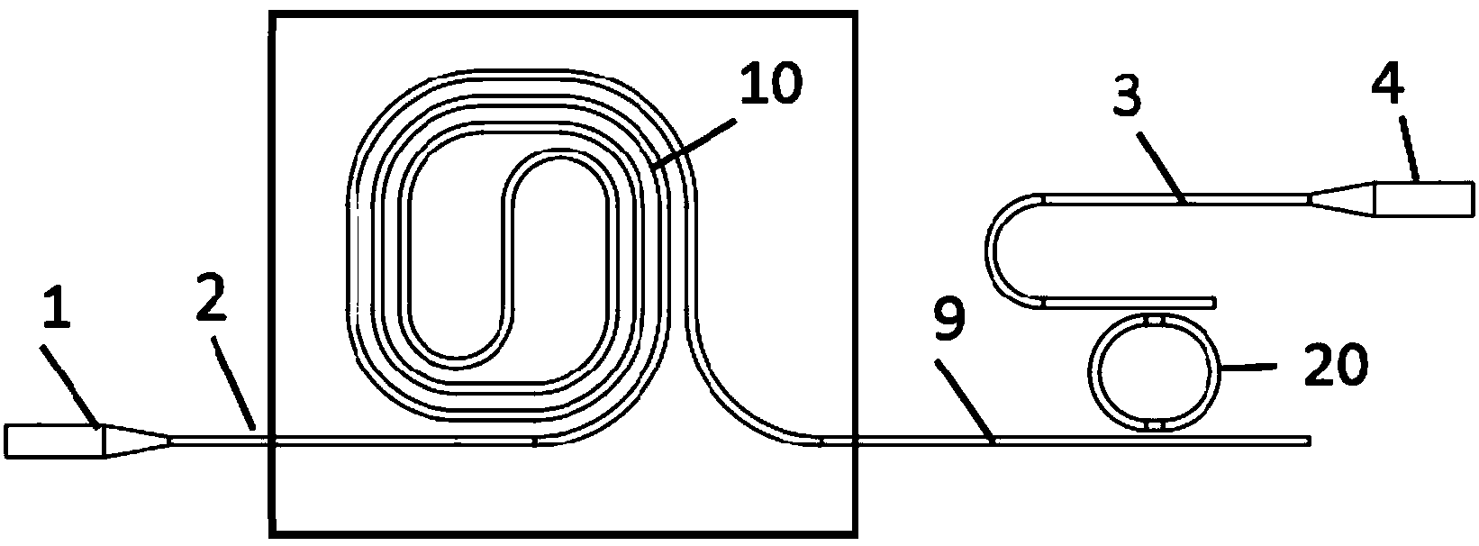
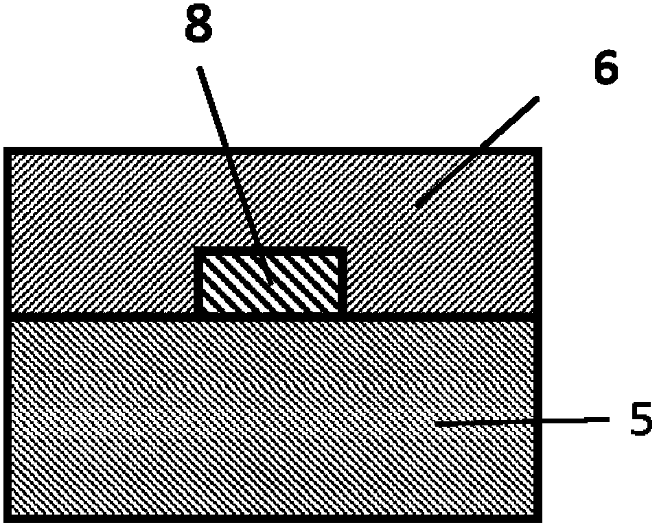
[0042] Such as figure 1 As shown, the present invention includes a wavelength tunable laser 1, an input waveguide 2, a spiral sensing waveguide 10, a connecting waveguide 9, a filter 20, an output waveguide 3 and an optical power meter 4, and the above wavelength tunable laser 1, input waveguide 2 , the spiral sensing waveguide 10 , the filter 20 , the connecting waveguide 9 , the output waveguide 3 and the optical power meter 4 are all located on the same substrate, between the waveguide lower cladding layer 5 and the waveguide upper cladding layer 6 .

[0043] The filter 20 adopts a ring resonator with a single microring structure, the optical power meter 4 adopts an integrated optical detector, and the wavelength tunable laser 1 is an integrated semiconductor wavelength tunable laser. The input waveguide 2, the helical sensing waveguide 10, the connecting waveguide 9, the output waveguide 3 and the filter 20 all adopt planar optical waveguides.

[0044] The waveguide upper...

Embodiment 2

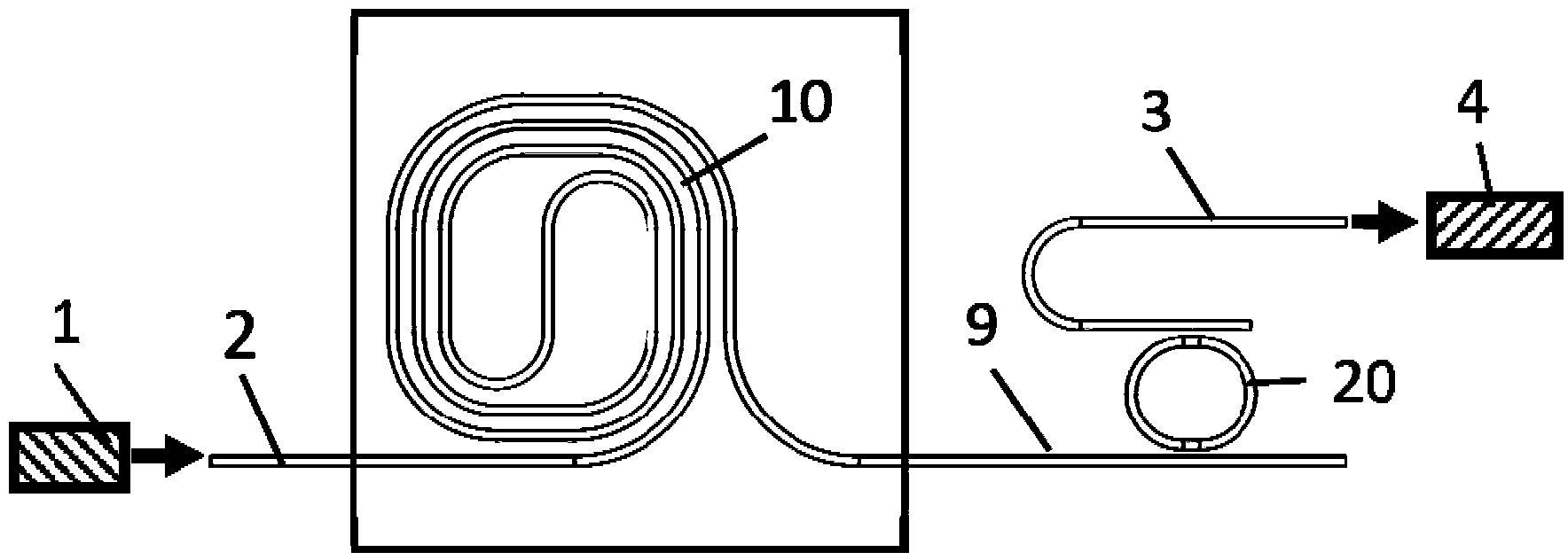
[0048] Such as figure 2 Shown, the present invention input waveguide 2, spiral sensing waveguide 10, connection waveguide 9, filter 20 and output waveguide 3, above-mentioned input waveguide 2, spiral sensing waveguide 10, filter 20, connection waveguide 9 and output The waveguides 3 are all located on the same substrate, between the waveguide lower cladding layer 5 and the waveguide upper cladding layer 6 .

[0049] The filter 20 adopts a single microring resonant cavity structure, and the input waveguide 2, the spiral sensing waveguide 10, the connecting waveguide 9, the output waveguide 3 and the filter 20 all adopt planar optical waveguides.

[0050] The waveguide upper cladding 6 of the spiral sensing waveguide 10 is removed, so that the waveguide core layer 8 is in contact with the detection sample 7 to realize detection, and the input end of the spiral sensing waveguide 10 is connected to an external wavelength tunable laser through the input waveguide 2, The output e...


PUM


Abstract

The invention discloses a Raman spectrum based optical waveguide sensor. The Raman spectrum based optical waveguide sensor comprises an input waveguide, a spiral sensing waveguide, a filter, a connecting waveguide and an output waveguide, wherein a detection window is formed in an upper cladding layer of the spiral sensing waveguide, the input end of the spiral sensing waveguide is connected with a wavelength tunable laser by the input waveguide, the output end of the spiral sensing waveguide is connected with one side of the filter by the connecting waveguide, and the other side of the filter is connected with an optical power meter by the output waveguide. The Raman spectrum based optical waveguide sensor can qualitatively analyze a single sample or a gas-liquid mixed sample, utilizes the planar optical waveguide as a Raman spectrum excitation and collection medium, and is integrated with the filter to obtain a small, low-cost and untagged sensor.

Description

technical field [0001] The invention is an optical waveguide sensor and relates to an optical waveguide sensor based on Raman spectrum. Background technique [0002] As an important field of information science, optical sensing technology has very important applications in environmental monitoring, pharmaceutical research and development, food safety and other fields. Optical waveguide sensors have the advantages of high sensitivity, anti-electromagnetic interference, easy integration, and real-time monitoring, and have been rapidly developed and widely used. [0003] The basic principle of the optical waveguide sensor device is that part of the light propagating in the optical waveguide is transmitted in the cladding of the optical waveguide in the form of evanescent waves. When the measured object is in contact with the optical fiber or the core layer of the planar waveguide, it will interact with the evanescent wave. , so as to change the characteristics of the light tra...

Claims


Application Information

Patent Timeline
Patent Type & Authority Applications(China)
IPC IPC(8): G01N21/65
Inventor 何建军江先鑫杨畅
Owner ZHEJIANG UNIV
Learn More