
SiC MOS (metal oxide semiconductor) capacitor and manufacturing method

A manufacturing method and capacitor technology, applied in semiconductor/solid-state device manufacturing, circuits, electrical components, etc., can solve the problems of large gate leakage current and cannot effectively reduce the interface state density of the device, so as to reduce the gate leakage current and improve the The effect of withstand voltage and reliability improvement

Inactive Publication Date: 2014-09-10
XIDIAN UNIV
View PDF5 Cites 9 Cited by
  • Summary
  • Abstract
  • Description
  • Claims
  • Application Information

AI Technical Summary

Problems solved by technology

Use high-k dielectric materials, such as HfO 2 , Al 2 o 3 instead of SiO 2 Layer is used as the dielectric material of MOS devices. Although this method improves the withstand voltage capability of the dielectric layer to a certain extent, this process cannot effectively reduce the interface state density of the device, and the traps introduced by high-k materials lead to excessive gate leakage current. Due to the gate leakage current limits the gate dielectric to withstand a higher electric field

Method used

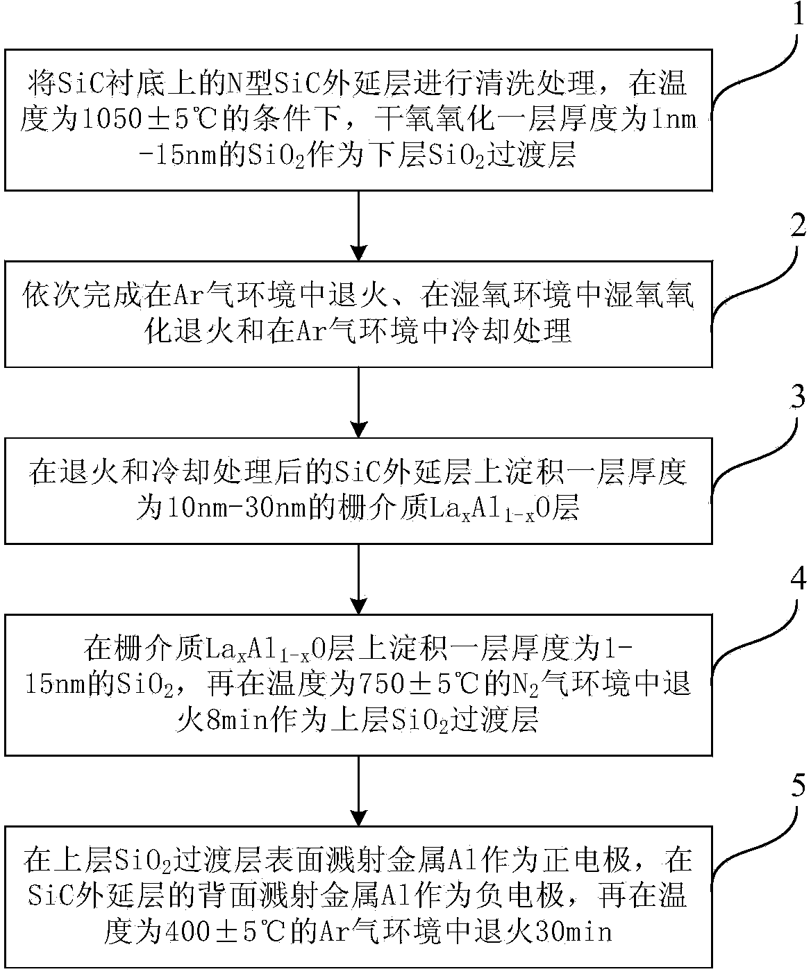

Image

  • SiC MOS (metal oxide semiconductor) capacitor and manufacturing method
  • SiC MOS (metal oxide semiconductor) capacitor and manufacturing method

Examples


Embodiment Construction

[0028] The technical solutions of the present invention will be described in further detail below with reference to the accompanying drawings and embodiments.

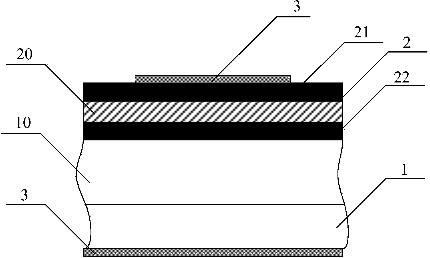
[0029] figure 1 It is a schematic diagram of a SiC MOS capacitor of the present invention. As shown in the figure, the present invention includes: a SiC substrate 1 , a gate dielectric layer 2 and positive and negative electrodes 3 .

[0030] Specifically, a SiC extension layer 10 is provided on the SiC substrate layer 1;

[0031] The gate dielectric layer 2 includes an upper layer of SiO 2 Transition layer 21, La x al 1-x O layer 20 and the underlying SiO 2 Transition layer 22; SiC epitaxial layer 10 is provided with lower layer SiO 2 Transition layer 22, lower layer SiO 2 The transition layer 22 is provided with La x al 1-x O layer 20, La x al 1-x O layer 20 is provided with upper layer SiO 2 Transition layer 21.

[0032] The positive and negative electrodes 3 are respectively connected with the upper lay...


PUM

PropertyMeasurementUnit
Thicknessaaaaaaaaaa
Doping concentrationaaaaaaaaaa
Thicknessaaaaaaaaaa

Abstract

The invention relates to a SiC MOS (metal oxide semiconductor) capacitor and a manufacturing method. The SiC MOS capacitor comprises a SiC substrate, a gate medium layer and positive and negative electrodes. A SiC extension layer is arranged on the SiC substrate. The gate medium layer comprises an upper SiO<2> transition layer, a La<x>Al<1-x>O medium layer and a lower SiO<2> transition layer, the lower SiO<2> transition layer is arranged on the SiC extension layer and is provided with the La<x>Al<1-x>O layer, and the upper SiO<2> transition layer is arranged on the La<x>Al<1-x>O layer, and the positive and negative electrodes are respectively connected with the surface of the upper SiO<2> transition layer and the back of the SiC substrate. The SiC substrate is an N-type heavy-dope SiC substrate, and the SiC extension layer is an N-type light-dope SiC extension layer. Accordingly, gate leak current is reduced, and voltage endurance and reliability of devices are improved.

Description

technical field [0001] The invention relates to a SiC MOS capacitor and a manufacturing method, in particular to a SiO 2 / La x al 1-x O / SiO 2 SiC MOS capacitance and manufacturing method of composite gate dielectric. Background technique [0002] As a typical representative of the third-generation semiconductor, SiC material has become an ideal material for making high-temperature, high-power, high-frequency and high-radiation-resistant devices due to its excellent physical and chemical properties. Compared with the first-generation semiconductor materials represented by Si and the second-generation semiconductor materials represented by GaAs, SiC materials have the advantages of large band gap, high critical breakdown electric field, and high thermal conductivity. Therefore, SiC materials and devices are currently , Process research and development has become a hot spot in the field of microelectronics technology research. Compared with other wide-bandgap semiconductor...

Claims


Application Information

Patent Timeline
IPC IPC(8): H01L29/94H01L21/02
CPCH01L29/94H01L21/02164H01L21/02172H01L21/022H01L29/6606
Inventor 贾仁需闫宏丽宋庆文汤晓燕张玉明
Owner XIDIAN UNIV
Learn More