Graphite bearing plate for processing LED epitaxial wafer

A technology for carrying discs and wafers, used in crystal growth, single crystal growth, from chemically reactive gases, etc.

Inactive Publication Date: 2014-09-17
XIAMEN SANAN OPTOELECTRONICS TECH CO LTD
View PDF7 Cites 19 Cited by
  • Summary
  • Abstract
  • Description
  • Claims
  • Application Information

AI Technical Summary

Problems solved by technology

[0005]Using the above-mentioned epitaxial wafer manufacturing process of the traditional graphite carrier plate, taking gallium nitride-based LED as an example, the following problems generally exist: (1) due to the growth on the sapphire substrate The LED wafer on the LED wafer has large lattice mismatch and thermal mismatch, and the sapphire substrate with a larger size (such as 4 inches or more) will have serious warping during the epitaxial process, resulting in the flat edge of the substrate being suspended. , so that the temperature of the flat side area is low, coupled with the serious air flow disturbance, it is easy to cause problems such as long flat side wavelength, poor wavelength uniformity, and high surface defect density; (2) In the MOCVD reaction chamber, due to the high speed of the graphite carrier during the growth process Rotation (speed 500~1200RPM), coupled with centrifugal force, one side of the substrate on the groove of the graphite carrier plate will be close to the graphite carrier plate, resulting in high temperature in the local area of ​​the edge, short wavelength or even no light, resulting in uniform wavelength poor performance, low surface yield, low chip yield, etc. 2)

Method used


Image

  • Graphite bearing plate for processing LED epitaxial wafer
  • Graphite bearing plate for processing LED epitaxial wafer
  • Graphite bearing plate for processing LED epitaxial wafer

Examples


Embodiment

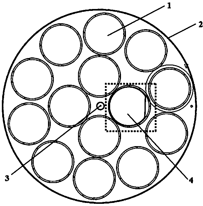
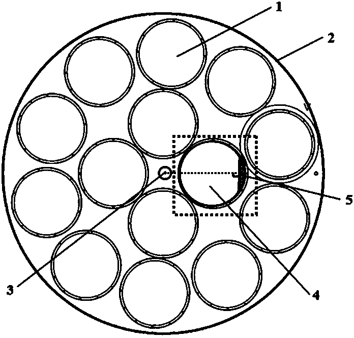
[0038] refer to Figure 3~Figure 6 As shown, a graphite carrier plate for LED epitaxial wafer manufacturing process, including: 14 4-inch (about 100.7mm in diameter) wafer grooves 1, the edge 2 of the graphite carrier plate and the shaft hole set in the center of the graphite carrier plate 3, wherein the wafer groove 1 is arranged above the carrier plate for placing a wafer substrate 4 with a flat edge (for convenience of illustration, only a wafer substrate in a wafer groove is shown in the figure), and A baffle structure 5 is provided on the inner edge 6 of the wafer groove, and the baffle is in a complementary relationship with the wafer substrate, and the two form a circle with the flat sides of the baffle and the wafer substrate as coincident sides.

[0039] In order to form a complementary relationship with the wafer substrate with flat sides, the shape of the baffle can be crescent-shaped or fan-shaped. In this embodiment, the crescent shape is preferred, and the circul...


PUM

PropertyMeasurementUnit
diameteraaaaaaaaaa

Abstract

The invention aims to provide a graphite bearing plate for processing an LED epitaxial wafer. The graphite bearing plate comprises a plurality of wafer grooves arranged above the bearing plate and used for holding epitaxial wafer substrates, wherein the inner side edge of each wafer groove is provided with a baffle structure, a baffle is in complementary relation with each wafer substrate, the wafer groove and the baffle structure are formed into an approximate roundness by taking the plat edges of the baffle and the wafer substrate as superposed edges, and the baffle structures can be used for reducing the gap position of the flat edges of the wafer substrates in the wafer grooves in an epitaxial growth process and ensuring the temperature and airflow stability of the flat edges of the wafer substrates, so that the edge yield of the epitaxial wafer substrates is increased.

Description

technical field [0001] The invention belongs to the technical field of semiconductors, and in particular relates to a graphite carrier plate used in an LED epitaxial wafer manufacturing process. Background technique [0002] Light Emitting Diode (English for Light Emitting Diode, referred to as LED) is a solid-state semiconductor diode light-emitting device, which is widely used in lighting fields such as indicator lights and display screens. [0003] At present, LED epitaxy (Epitaxy in English) wafers are mostly obtained by Metal-organic Chemical Vapor Deposition (Metal-organic Chemical Vapor Deposition in English, MOCVD for short). bottom) into the groove of the graphite carrier (wafer carrier in English), and together with the graphite carrier, it is introduced into the MOCVD reaction chamber. The substrate and the graphite carrier are heated to a high temperature of about 1000°C, and the organic Metal compounds and Group V gases are repolymerized on the wafer substrate ...

Claims


Application Information

Patent Timeline
Patent Type & Authority Applications(China)
IPC IPC(8): C30B25/12
Inventor 郑锦坚周启伦寻飞林伍明跃邓和清李志明李水清
Owner XIAMEN SANAN OPTOELECTRONICS TECH CO LTD
Why Eureka
Try Eureka