Polysilicon resistor integration production method in silicon-germanium HBT (Heterojunction Bipolar Transistor) process

A technology of polysilicon resistors and manufacturing methods, which is applied in the direction of resistors, circuits, electrical components, etc., can solve problems affecting the uniformity of polysilicon resistance, base polysilicon residues, defects, etc., to reduce the possibility of polysilicon residues, prevent damage or The effect of falling off and increasing the slope

Active Publication Date: 2014-09-24
SHANGHAI HUAHONG GRACE SEMICON MFG CORP
View PDF3 Cites 4 Cited by
  • Summary
  • Abstract
  • Description
  • Claims
  • Application Information

AI Technical Summary

Problems solved by technology

like Figure 1C As shown, the silicon oxide residue 107B becomes a barrier layer during the subsequent etching of the polysilicon, that is, the silicon germanium epitaxial layer 106 and the polysilicon seedling 105, resulting in the base polysilicon residue 105a along the polysilicon resistor, which is then cleaned during subsequent ultrasonic cleaning. Become a defect and affect the uniformity of polysilicon resistance

Method used


Image

  • Polysilicon resistor integration production method in silicon-germanium HBT (Heterojunction Bipolar Transistor) process
  • Polysilicon resistor integration production method in silicon-germanium HBT (Heterojunction Bipolar Transistor) process
  • Polysilicon resistor integration production method in silicon-germanium HBT (Heterojunction Bipolar Transistor) process

Examples


Embodiment Construction

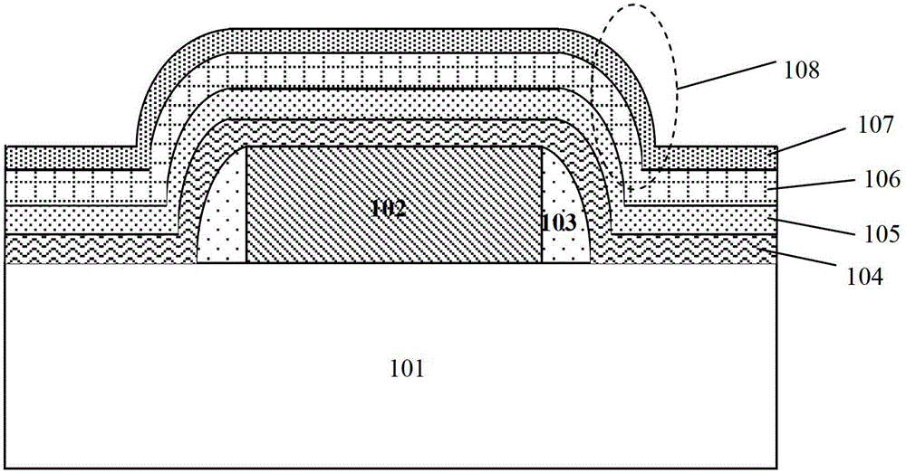
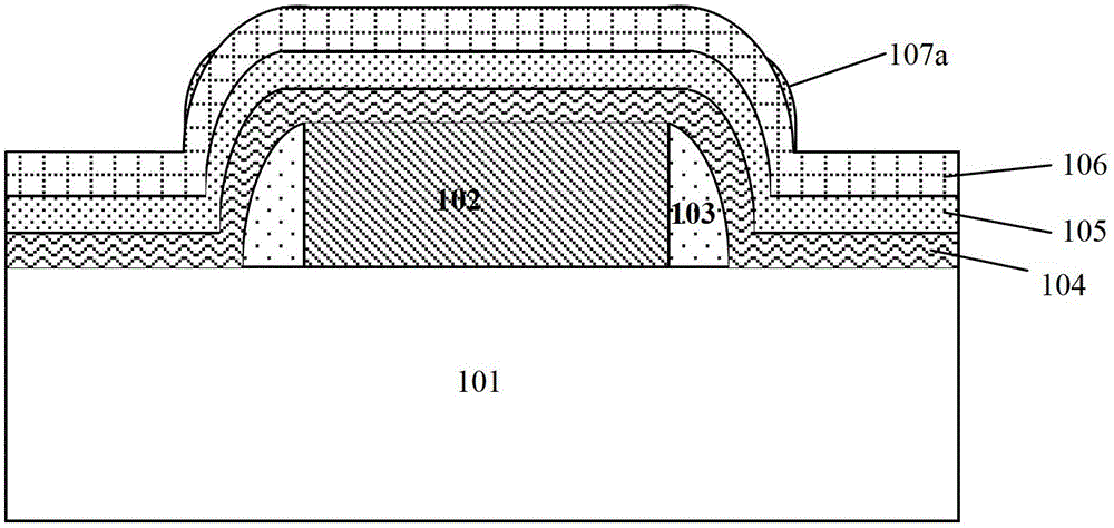
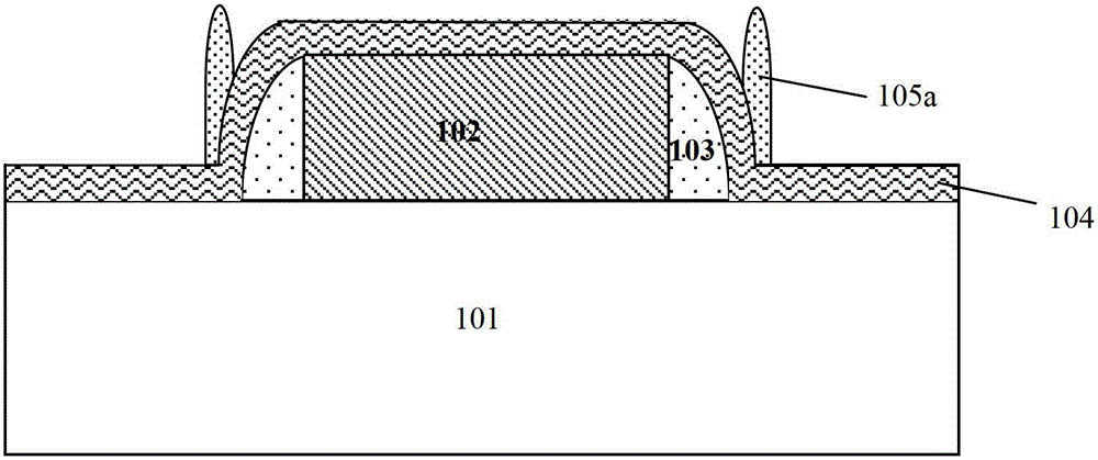
[0036] like figure 2 Shown is the flow chart of the method of the embodiment of the present invention; Figure 3A to Figure 3E Shown is a schematic diagram of the device structure in each step of the method of the embodiment of the present invention. The polysilicon resistance integrated manufacturing method in the silicon germanium HBT process of the embodiment of the present invention is used to realize the integrated production of the polysilicon resistance 2 and the silicon germanium HBT, including the following steps:

[0037] Step 1, such as Figure 3A As shown, a silicon substrate with a field oxygen 1 isolation structure is provided, and an active region of the silicon substrate is isolated by the field oxygen 1 . The field oxygen 1 is local field oxygen (LOCOS) or shallow trench oxygen (STI). Figure 3A The structure diagram of the formation region of the polysilicon resistor 2 is only shown in the figure, and the structure diagram of the formation region of the sil...


PUM


Abstract

The invention discloses a polysilicon resistor integration production method in a silicon-germanium HBT process. The method includes the steps of depositing a first polysilicon layer and doping; performing photolithographic etching on the first polysilicon layer to form a polysilicon resistor; depositing a second silicon oxide layer and performing reverse etching on the second silicon oxide layer to form a sidewall of the polysilicon resistor; using a thermal oxidation process to form a third silicon oxide layer; depositing a fourth silicon oxide layer and a fifth polysilicon sub-crystal layer sequentially; using a photolithography process and an etching process to open the window of an epitaxial layer of the silicon-germanium; depositing an epitaxial layer of the silicon-germanium and a sixth silicon oxide layer; using the photolithographic process to define a formation area of the base area of a silicon-germanium HBT; using a wet etching process to remove the sixth silicon oxide layer outside the base area; using a dry etching process to remove the silicon-germanium epitaxial layer outside the base area and the fifth polysilicon sub-crystal layer and forming the base area. The polysilicon resistor integration production method in the silicon-germanium HBT process can eliminate the residual polysilicon on the periphery of the polysilicon resistor to improve the surface uniformity of the polysilicon resistor.

Description

technical field [0001] The invention relates to a semiconductor integrated circuit manufacturing process method, in particular to a polysilicon resistor integrated manufacturing method in a silicon germanium (SiGe) heterojunction bipolar transistor (Heterojunction bipolar transistor, HBT) process. Background technique [0002] The RF front-end chip circuit used in the communication field generally consists of four parts: power amplifier, low noise amplifier, switch circuit and simple logic control circuit. The power silicon germanium HBT process, after integrating SiGe NPN, PNP, resistors, capacitors (including variable capacitors), inductors and switching devices, can meet the requirements of on-chip matching, logic control and transceiver conversion in the circuit. [0003] On the basis of the silicon germanium HBT process, it is very important to integrate various devices and obtain better uniformity and a larger process window. Capacitors and inductors are separate devi...

Claims


Application Information

Patent Timeline
Patent Type & Authority Applications(China)
IPC IPC(8): H01L21/822H01L21/02
CPCH01L21/8222H01L28/20H01L29/66242
Inventor 陈曦周正良陈帆潘嘉
Owner SHANGHAI HUAHONG GRACE SEMICON MFG CORP
Why Eureka
Try Eureka