Bismuth-replacement RIG (rare earth iron garnet) monocrystal and manufacturing method thereof
An iron garnet, bismuth replacement technology, applied in the direction of single crystal growth, single crystal growth, chemical instruments and methods, etc., can solve problems such as oscillation instability, achieve small environmental impact, excellent crystallinity, and less Pt and Pb content Effect
- Summary
- Abstract
- Description
- Claims
- Application Information
AI Technical Summary
Problems solved by technology
Method used
Image

Examples
Embodiment 1
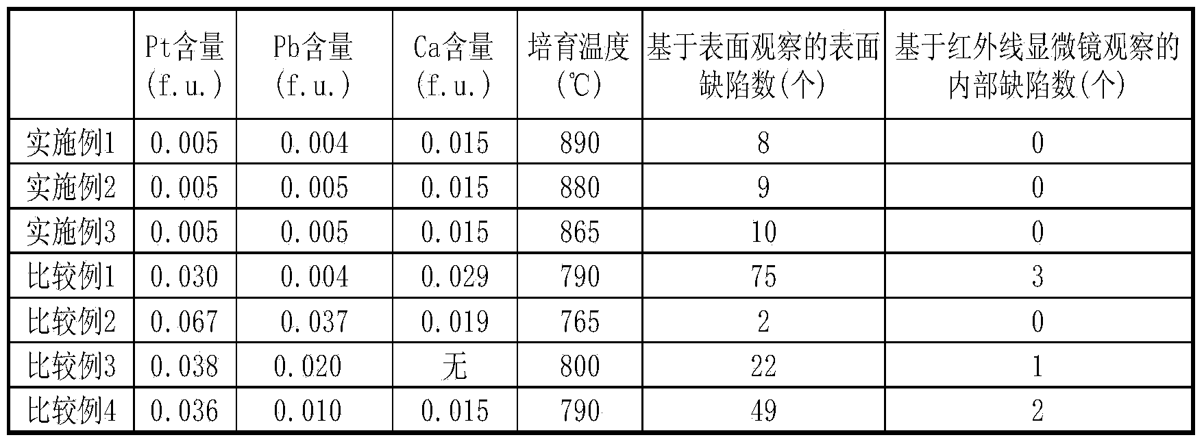
[0075] In the Pt crucible, 80% by mass of bismuth oxide (Bi 2 o 3 ), 0.9% by mass of boron oxide (B 2 o 3 ), 9.7% by mass of lead oxide (PbO), 0.013% by mass of calcium oxide (CaO), 7.8% by mass of iron oxide (Fe 2 o 3 ), 0.67% by mass of gallium oxide (Ga 2 o 3 ), 0.65% by mass of terbium oxide (Tb 4 o 7 ) and 0.27% by mass of ytterbium oxide (Yb 2 o 3 ), to prepare melt raw materials.
[0076] Arrange the Pt crucible with the prepared melt raw materials in a precision vertical tubular electric furnace, heat to 1000°C to melt, stir fully, and mix evenly to form a RIG cultivation melt. Next, the temperature of the melt was lowered to 890° C. below the saturation temperature (905° C.), and a (111) garnet single crystal having a diameter of 3 inches, a thickness of 760 μm, and a lattice constant of 1.2497 nm was obtained. [(GdCa) 3 (CaMgZr) 5 o 12 ] One side of the substrate is in contact with the melt surface.
[0077] In an air atmosphere, epitaxial growth was p...
Embodiment 2
[0083] The RIG single crystal was grown under the same conditions as in Example 1 except that the RIG single crystal was grown at 880°C.
[0084] The grown RIG single crystal had a diameter of 3 inches and a film thickness of 530 μm. The crystal growth rate was 0.260 μm / min. As a result of microscopic observation of the entire surface of the grown RIG single crystal, nine crystal defects were confirmed, but no damage such as cracks was found in the RIG.
[0085] The grown RIG single crystal was cut into 11 mm squares, the substrate was removed by grinding, and both sides were mirror-polished by chemical mechanical polishing (CMP) to obtain a RIG single crystal with a thickness of 450 μm.
[0086] The internal pits (crystal defects) of the mirror-polished RIG single crystal of 11 mm square were observed with an infrared microscope, and as a result, no crystal defects were confirmed.
[0087] The composition of the mirror-polished RIG single crystal was analyzed by X-ray fluor...
Embodiment 3
[0090] The RIG single crystal was grown under the same conditions as in Example 1 except that the RIG single crystal was grown at 865°C.
[0091] The grown RIG single crystal had a diameter of 3 inches and a film thickness of 530 μm. The crystal growth rate was 0.260 μm / min. As a result of microscopic observation of the entire surface of the grown RIG single crystal, 10 crystal defects were confirmed, but no damage such as cracks was found in the RIG.
[0092] The grown RIG single crystal was cut into 11 mm squares, the substrate was removed by grinding, and both sides were mirror-polished by chemical mechanical polishing (CMP) to obtain a RIG single crystal with a thickness of 450 μm.
[0093] The internal pits (crystal defects) of the mirror-polished RIG single crystal of 11 mm square were observed with an infrared microscope, and as a result, no crystal defects were confirmed.
[0094] The composition of the mirror-polished RIG single crystal was analyzed by X-ray fluores...
PUM
| Property | Measurement | Unit |
|---|---|---|
| Film thickness | aaaaa | aaaaa |
| Thickness | aaaaa | aaaaa |
| Film thickness | aaaaa | aaaaa |
Abstract
Description
Claims
Application Information
 - R&D
- Intellectual Property
- Life Sciences
- Materials
- Tech Scout
- Unparalleled Data Quality
- Higher Quality Content
- 60% Fewer Hallucinations
Browse by: Latest US Patents, China's latest patents, Technical Efficacy Thesaurus, Application Domain, Technology Topic, Popular Technical Reports.
© 2025 PatSnap. All rights reserved.Legal|Privacy policy|Modern Slavery Act Transparency Statement|Sitemap|About US| Contact US: help@patsnap.com