A Method for Detecting Etched Sidewall Roughness Using Capacitance Change

A technology of sidewall roughness and capacitance change, applied in the field of ion etching technology, can solve the influence of the electrical performance of devices that cannot directly reflect the sidewall roughness, cannot accurately predict the sidewall roughness, and is difficult to change the sidewall roughness, etc. problem, to avoid electrical fatigue, easy to operate, to achieve the effect of simplicity

Inactive Publication Date: 2016-12-07
PEKING UNIV +1
View PDF5 Cites 0 Cited by
  • Summary
  • Abstract
  • Description
  • Claims
  • Application Information

AI Technical Summary

Problems solved by technology

Due to the complexity of the plasma model and the etching reaction model, it is theoretically impossible to accurately predict the specific roughness of the sidewall under different etching conditions. At the same time, it is difficult to monitor the etching in real time because the etching process takes place in the closed cavity of the equipment. Variations in sidewall roughness during
[0003] Previous studies often focused on the verticality of the sidewall of the etched deep groove and the roughness of the bottom surface of the deep groove, and the roughness of the sidewall was often neglected. The inspection was generally carried out by observing the cross-section of the device structure with an electron microscope, and estimating the roughness by using electron microscope photos. , this method can be applied to structures with large size and low aspect ratio, but for structures with small size and high aspect ratio, the acquisition of the cross section is easy to destroy the functional structure, and it is easy to cause non-etched sidewall roughness , and as the complexity of the device structure increases, there will be different etching windows on the same silicon wafer, and the sidewall roughness of a section cannot reflect the sidewall roughness formed under other etching conditions. It cannot directly reflect the influence of sidewall roughness on the electrical performance of the device

Method used


Image

  • A Method for Detecting Etched Sidewall Roughness Using Capacitance Change
  • A Method for Detecting Etched Sidewall Roughness Using Capacitance Change
  • A Method for Detecting Etched Sidewall Roughness Using Capacitance Change

Examples


Embodiment 1

[0040] The method for detecting the roughness of the etched side wall by using the capacitance change in this embodiment is specifically implemented as follows: Figure 1(a) ~ Figure 1(g) As shown, the specific description is as follows:

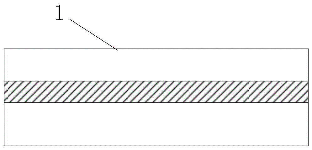
[0041] 1. Preparation: SOI substrate 1 is used as the substrate of the chip, as shown in FIG. 1( a ).

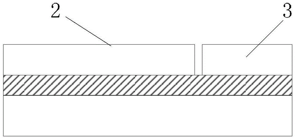
[0042] 2. Use MEMS process photolithography on the substrate to define the detection area 3, and use the etching process to isolate the detection area 3 and the functional area 2, including: DRIE Si As shown in Figure 1(b).

[0043] The etching depth value is the thickness of the silicon layer on the front side of the SOI silicon wafer, and the front side silicon layer is etched through the etching process to realize the electrical insulation between the detection area 3 and the functional area 2 .

[0044] That is to say, in the present invention, the functional area and the detection area of ​​the device are isolated by the buried oxi...


PUM


Abstract

The invention discloses a method for detecting the roughness of the etched side wall by using the capacitance change. The above-mentioned process flow is only added before the etching process in the functional area, so as to avoid increasing the complexity of the design of the functional device; the capacitance change of the detection area is used to reflect the side wall of the functional area Roughness, which reduces the error caused by the small size, and avoids operations that damage the device structure such as fractures, and realizes non-destructive testing of the etched structure; the number of detection areas is determined by the size of the etching window in the functional area, achieving a more Accurately detect the purpose of etching sidewall roughness under different conditions, and at the same time realize one-step detection of sidewall roughness under different etching conditions. The technological process designed by the invention is simple, each process is a mature technology, the technological difficulty is relatively low, and the realization is simple and easy to operate.

Description

technical field [0001] The invention belongs to the field of micro-electro-mechanical system (MEMS) processing technology, and is particularly applied to the plasma etching technology in the etching process. By designing an independent detection area, the capacitance measurement of the detection structure is used to reflect the roughness of the side wall in the etching process. Background technique [0002] The etching process is a very important single process in the MEMS processing technology, and an indispensable technical means to realize the functional structure of the micro-electro-mechanical system. The etching process in the current MEMS processing technology is mainly divided into isotropic etching and anisotropic etching. Isotropic etching is mainly used in large-size, spherical structures that do not have high requirements for body-to-width ratios, and sidewall roughness generally has little impact on such devices. Anisotropic etching is mainly used in deep groov...

Claims


Application Information

Patent Timeline
Patent Type & Authority Patents(China)
IPC IPC(8): G01B7/34
Inventor 张立何军张大成黄贤赵丹淇王玮杨芳田大宇刘鹏李婷罗葵
Owner PEKING UNIV
Why Eureka
Try Eureka