Method for forming gate electrode

A gate and dummy gate technology, applied in electrical components, circuits, semiconductor devices, etc., can solve the problems of poor performance of MOS transistors and affecting the shape of metal gates, etc., and achieve the effect of easy control of width and formation position

Active Publication Date: 2014-10-15
SEMICON MFG INT (SHANGHAI) CORP
View PDF3 Cites 6 Cited by
  • Summary
  • Abstract
  • Description
  • Claims
  • Application Information

AI Technical Summary

Problems solved by technology

However, in the subsequent high-temperature process, such as the impurity activation process or film deposition process after ion implantation in the source and drain regions, the gate dielectric layer 101, the protective layer 102 and the dummy gate 103 will be different degrees The shrinkage of the gate dielectric layer 101 causes the width of the gate dielectric layer 101 to be smaller than the width of the dummy gate 103, which affects the morphology of the subsequent metal gate formation, resulting in poor performance of the MOS transistor

Method used


Image

  • Method for forming gate electrode
  • Method for forming gate electrode
  • Method for forming gate electrode

Examples


no. 1 example

[0036] Figure 2 to Figure 8 is a schematic cross-sectional structure diagram of the formation process of the gate in the first embodiment of the present invention.

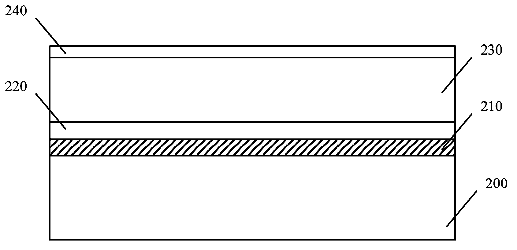
[0037] Please refer to figure 2 A semiconductor substrate 200 is provided, the surface of the semiconductor substrate 200 has a gate dielectric material layer 210 , the gate dielectric material layer 210 has a protective material layer 220 thereon, and the protective material layer 220 has a dummy gate material layer 230 thereon.

[0038] The semiconductor substrate 200 may be silicon or silicon-on-insulator (SOI), and the semiconductor substrate 200 may also be germanium, silicon germanium, gallium arsenide, or germanium-on-insulator. In this embodiment, the semiconductor substrate 200 is a silicon substrate. The semiconductor substrate 200 serves as a working platform for subsequent processes.

[0039] The surface of the semiconductor substrate 200 has a gate dielectric material layer 210, the gate dielectr...

no. 2 example

[0058] Figure 9 to Figure 16 is a schematic cross-sectional structure diagram of the formation process of the gate in the second embodiment of the present invention.

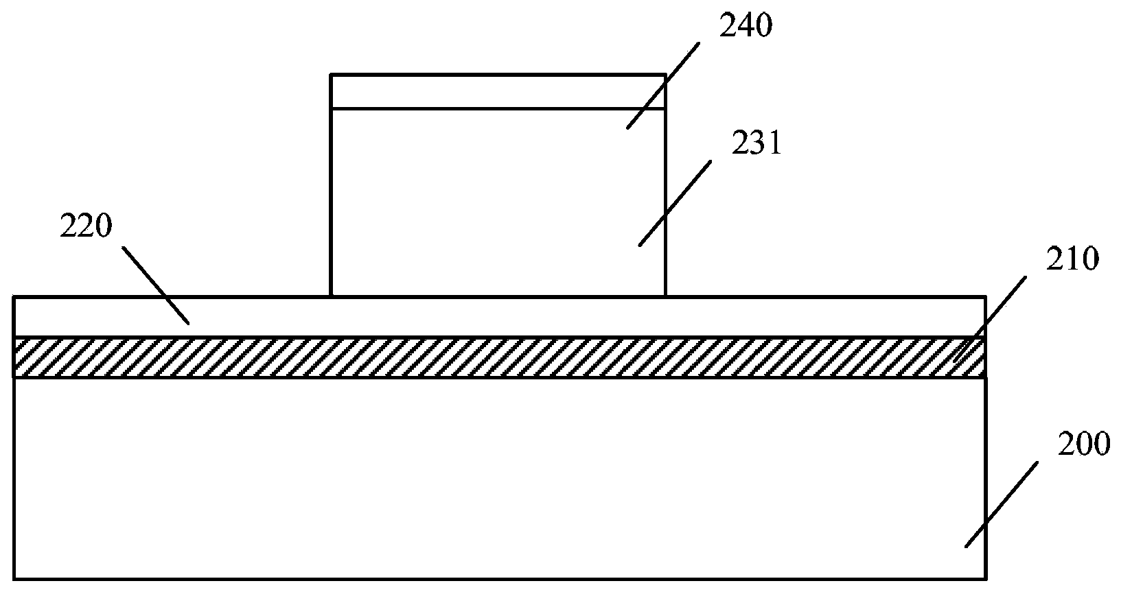
[0059] Please refer to Figure 9 , provide a semiconductor substrate 300, the semiconductor substrate 300 has a first region I and a second region II, the surface of the semiconductor substrate 300 has a gate dielectric material layer 310, and the gate dielectric material layer has a protective material layer 320 , the protective material layer 320 has a dummy gate material layer 330 on it.

[0060] In this embodiment, the dummy gate material layer 330 is a polysilicon layer, the material of the protection layer 320 is a titanium nitride layer, the gate dielectric material layer 310 is a high dielectric constant material, and the high dielectric constant material for HfO 2 , ZrO 2 、Al 2 o 3 , HfSiO, HfSiON, HfTaO and one or more of HfZrO. In this embodiment, a hard mask layer 340 is further formed on the...


PUM


Abstract

A method for forming a gate electrode includes the following steps: a semiconductor substrate is provided, the surface of the semiconductor substrate has a gate medium material layer, a protection material layer is arranged on the gate medium material layer, and a pseudo gate material layer is arranged on the protection material layer; the pseudo gate material layer is etched, and a pseudo gate is formed on the protection material layer; a first side wall is epitaxially formed on a side wall surface of the pseudo gate; the protection material layer is etched using the pseudo gate and the first side wall as a mask, so as to form a protective layer, and the width of the protective layer is larger than that of the pseudo gate; a second side wall is epitaxially formed on a side wall surface of the first side wall; and the gate medium material layer is etched using the pseudo gate and the second side wall as a mask, so as to form a gate medium layer, and the width of the gate medium layer is larger than that of the protective layer. In the gate electrode formed in the invention, the gate medium layer, the protective layer and the pseudo gate are in a stepped structure, and the gate electrode has good performance.

Description

technical field [0001] The invention relates to the technical field of semiconductors, in particular to a method for forming a gate. Background technique [0002] As the feature size of semiconductor devices becomes smaller and smaller, the area occupied by core devices also decreases accordingly, resulting in a substantial increase in energy density per unit area, and the problem of leakage current becomes more prominent. Therefore, in the process below the 45nm node, the traditional process of using silicon dioxide material as the gate dielectric layer has encountered a bottleneck and cannot meet the process requirements of semiconductor devices. In order to solve the above problems, high dielectric constant (high-K) dielectric materials are generally used as the gate dielectric layer, and then a gate electrode of metal material is formed on the gate dielectric layer to form a high-K metal gate (HKMG) structure. reduce leakage current. [0003] Please refer to figure 1 ...

Claims


Application Information

Patent Timeline
Patent Type & Authority Applications(China)
IPC IPC(8): H01L21/28
CPCH01L29/42356H01L29/42364
Inventor 王新鹏
Owner SEMICON MFG INT (SHANGHAI) CORP
Why Eureka
Try Eureka