IGBT chip and preparation method thereof

A chip and control area technology, applied in semiconductor/solid-state device manufacturing, electrical components, circuits, etc., can solve the problems of increased difficulty in IGBT device design, achieve the effects of shortening extraction time, increasing switching speed, and alleviating conflicting relationships

Active Publication Date: 2014-11-19
ZHUZHOU CRRC TIMES SEMICON CO LTD
View PDF4 Cites 9 Cited by
  • Summary
  • Abstract
  • Description
  • Claims
  • Application Information

AI Technical Summary

Problems solved by technology

However, it is necessary to optimize the junction depth and doping concentration of the collector region in order to determine th

Method used


Image

  • IGBT chip and preparation method thereof
  • IGBT chip and preparation method thereof
  • IGBT chip and preparation method thereof

Examples


Embodiment Construction

[0050] Specific embodiments of the present invention will be described in detail below in conjunction with the accompanying drawings.

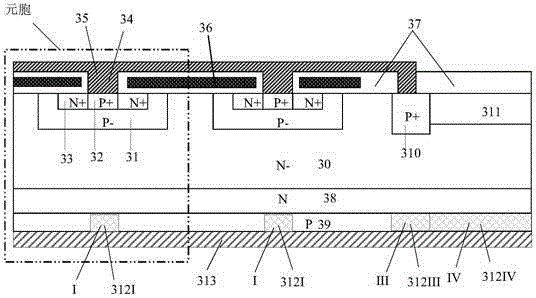
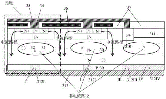
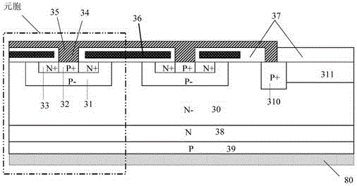
[0051] It should be noted that the structure of the IGBT chip provided by the present invention is based on the existing IGBT chip structure with a local minority carrier injection efficiency control area added. Therefore, the structure of the IGBT chip provided by the present invention is basically the same as that of the existing IGBT chip. The IGBT chip described in the embodiment of the present invention may have a planar gate structure or a trench gate structure, and the embodiment of the present invention takes the IGBT chip with a planar gate structure as an example for illustration. The specific structure of the IGBT chip with a planar gate structure is as follows: figure 2 with image 3 shown. figure 2 is a schematic top view structure diagram of an IGBT chip according to an embodiment of the present invention, image 3 is a sch...


PUM


Abstract

The invention provides an IGBT chip and a preparation method thereof. The IGBT chip comprises a chip front face and a chip back face. The chip front face comprises a cell area, a gate area, an equipotential ring area and a terminal structure area. The cell area comprises a plurality of mutually parallel cells. Each of the cells comprises an emitter electrode. The chip back face comprises a collector region, and a local minority injection efficiency control area is arranged in at least one corresponding collector area under the emitter electrode, a corresponding collector area under the gate area, a corresponding collector area under the equipotential ring area and/or a corresponding collector area under the terminal structure area. The local minority injection efficiency control area can control the minority injection efficiency in the area. Through the IGBT chip provided by the invention, the contradictory relationship between conduction loss and turn-off loss can be alleviated, and the reduction of the turn-off loss of the IGBT chip as far as possible in the condition of not increasing the conduction loss is realized.

Description

technical field [0001] The invention relates to the field of semiconductor devices, in particular to an IGBT chip with reduced power consumption and a preparation method thereof. Background technique [0002] An insulated gate bipolar transistor (IGBT) is a bipolar device. The structure of the IGBT device is as figure 1 As shown, the substrate of the IGBT device is made of N-type semiconductor material. It includes an N-base region 10 (substrate), an emitter P well 11 above the N-base region 10, an emitter ohmic contact P+ region 12, an N+ source region 13, and a buffer layer below the N-base region 10 14 and the collector region 15. Wherein, the emitter is located on the front side of the device, and the collector region 15 is located on the back side of the device. The hole carriers in this collector region are called minority carriers. [0003] When the device is turned on, the minority carriers in the collector region 15 are emitted and injected into the N-base regi...

Claims


Application Information

Patent Timeline
IPC IPC(8): H01L29/739H01L29/06H01L21/331
CPCH01L29/0821H01L29/66325H01L29/7393
Inventor 刘国友覃荣震黄建伟
Owner ZHUZHOU CRRC TIMES SEMICON CO LTD
Why Eureka
Try Eureka