Organic electroluminescent display (OLED), manufacturing method thereof and display device

An electroluminescence display and display panel technology, applied in circuits, electrical components, electrical solid devices, etc., can solve the problems affecting the uniformity of the film layer, uneven spreading, disconnection of the cathode 70, etc., to ensure the uniformity of the film layer. , Improve the luminous performance and avoid the effect of color mixing

Active Publication Date: 2014-11-26
BOE TECH GRP CO LTD
View PDF5 Cites 64 Cited by
  • Summary
  • Abstract
  • Description
  • Claims
  • Application Information

AI Technical Summary

Problems solved by technology

[0004] At present, there are mainly two structures for the pixel definition layer in OLEDs. One is to use a pixel definition layer whose cross-section is a positive trapezoid whose upper base is smaller than the lower base, such as Figure 1a As shown (only a part is shown in the figure), after the generally trapezoidal pixel-defining layer 10 is fabricated, in order to avoid the problem of color mixing in adjacent pixel regions, hydrophobic treatment is required to make the surface of the pixel-defining layer have hydrophobic properties. Although this can avoid the problem of color mixing, it is easy to make the light-emitting layer 20 made in the opening area of ​​the pixel defining layer spread unevenly, and cause the problem of tiny gaps 30 in the light-emitting layer 20. The short circuit between the cathode 40 and the anode 50 located under the light-emitting layer at the tiny gap 30
The other is to define the layer with pixels whose section is an inverted trapezoid whose upper base is larger than the lower base, such as Figure 1b As shown (only a part is shown in the figure), although the inverted trapezoidal pixel defining layer 60 can avoid the problem of short circuit between the cathode 70 and the anode 80, the inverted trapezoidal pixel defining layer 60 easily disconnects the cathode 70 formed later. The problem
[0005] Therefore, the structure of the above-mentioned existing pixel defining layer will affect the uniformity of the film layer formed later, and affect the light-emitting performance of the OLED.

Method used


Image

  • Organic electroluminescent display (OLED), manufacturing method thereof and display device
  • Organic electroluminescent display (OLED), manufacturing method thereof and display device
  • Organic electroluminescent display (OLED), manufacturing method thereof and display device

Examples


example 1

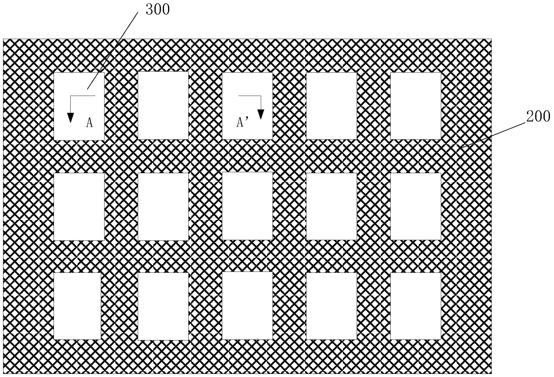
[0059] Example 1: If Figure 4 As shown, the specific steps for making an organic electroluminescent display panel are as follows:

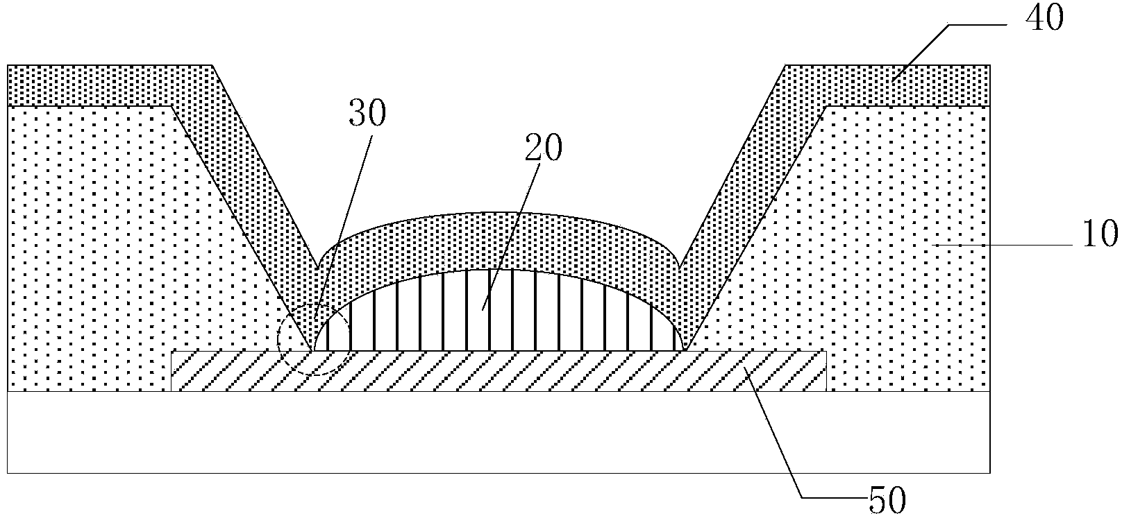
[0060] S201. Coating a layer of lyophobic material with a negative photoresist property on the base substrate 100, such as Figure 6a shown;

[0061] S202. Use the first mask to pattern the lyophobic material with negative photoresist properties by exposure, development and etching to form the pattern of the first pixel defining layer structure 210. At this time, because of the negative photoresist The lyophobic material of the glue nature is formed into a material insoluble in the developer after exposure, while the unexposed material dissolves in the developer, thereby forming the pattern of the first pixel defining layer structure, and because the negative photoresist As the thickness increases, the photoresist material closer to the base substrate receives less light intensity, so the pattern of the formed first pixel defining layer structu...

example 2

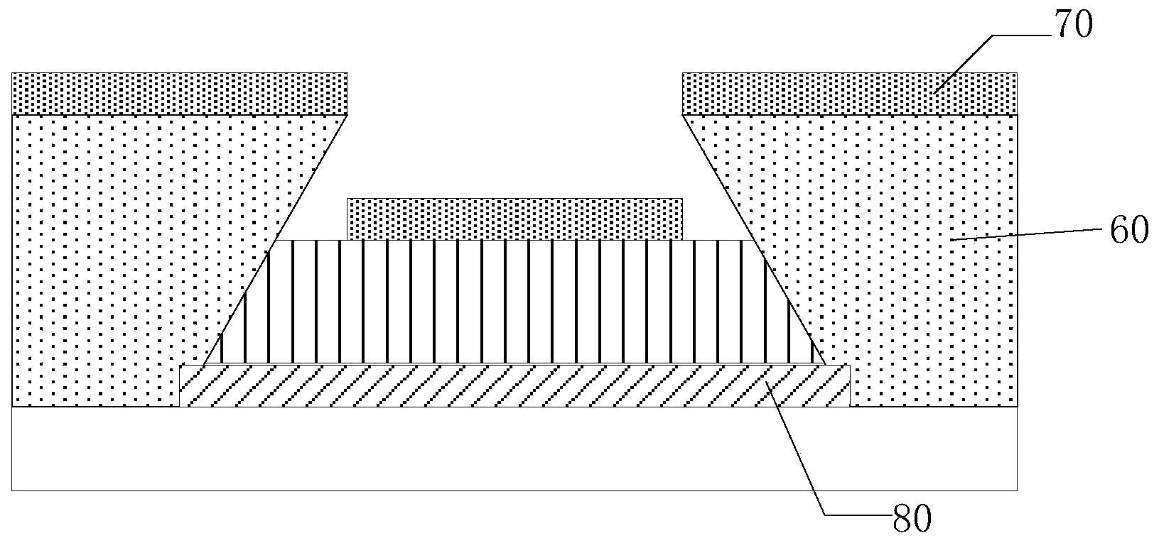
[0065] Example 2: If Figure 5 As shown, the specific steps for making the pixel defining layer of the organic electroluminescence display panel are as follows:

[0066] Steps S301 and S302 are completely the same as steps S201 and S202 in Example 1, and will not be repeated here.

[0067] S303, coating a layer of lyophilic material with positive photoresist properties on the base substrate 100 formed with the first pixel defining layer structure 210, at this time the lyophilic material completely covers the first pixel defining layer structure 210 , that is, the upper surface of the first pixel defining layer structure 210 is also covered with a lyophilic material, such as Figure 7a shown;

[0068] S304. Pattern the lyophilic material with positive photoresist properties, and form the pattern of the second pixel defining layer structure 220 by means of exposure, development and etching, wherein the first pixel defining layer structure 210 is covered during etching The lyo...


PUM


Abstract

The invention discloses an organic electroluminescent display (OLED), a manufacturing method of the organic electroluminescent display (OLED) and a display device. A pixel defining layer arranged in the organic electroluminescent display (OLED) is provided with opening areas corresponding to pixel areas of the OLED, an opening of each opening area is larger than the bottom face of the opening area, and thus the problem that a cathode may break later can be avoided; because the upper surface of the pixel defining layer is made from lyophobic material, and luminescent material with which the pixel defining layer is coated later cannot remain on the upper surface of the pixel defining layer easily, the problem that colors of the adjacent pixel areas are mixed can be avoided; meanwhile, the inclined faces of the corresponding opening areas of the pixel defining layer are made from lyophilic material so that it can be guaranteed that the opening areas are evenly filled with the luminescent material with which the pixel defining layer is coated later. Therefore, according to the OLED, the uniformity of a film layer formed later on the pixel defining layer can be guaranteed, and the luminescence property of the OLED is improved.

Description

technical field [0001] The present invention relates to the field of display technology, in particular to an organic electroluminescence display panel, a manufacturing method thereof and a display device. Background technique [0002] At present, organic electroluminescent display panel (Organic Electroluminescent Display, OLED) has gradually become the display field due to its characteristics of low power consumption, high color saturation, wide viewing angle, thin thickness, no need for backlight, and flexibility. mainstream. [0003] The basic structure of an OLED includes a substrate, an anode, a light-emitting layer, and a cathode arranged on the substrate in sequence. The holes will recombine in the light-emitting layer to form excitons, and excite the organic materials in the light-emitting layer to emit light; the light-emitting layer is made by inkjet printing technology. Generally, before making the light-emitting layer, it is necessary to make pixel definitions o...

Claims


Application Information

Patent Timeline
Patent Type & Authority Applications(China)
IPC IPC(8): H01L27/32H01L51/56H01L51/52
CPCH10K71/135H10K59/122H10K50/11H10K71/191H10K59/1201
Inventor 宋莹莹洪晓雯洪豪志
Owner BOE TECH GRP CO LTD
Why Eureka
Try Eureka