Inverted organic light emission diode and preparation method and application thereof

An electroluminescence device, an organic technology, applied in the field of electric light sources, can solve problems such as poor conductivity, difficulty in ensuring uniformity, and increased driving voltage

Inactive Publication Date: 2014-12-03
OCEANS KING LIGHTING SCI&TECH CO LTD +2
View PDF4 Cites 3 Cited by
  • Summary
  • Abstract
  • Description
  • Claims
  • Application Information

AI Technical Summary

Problems solved by technology

Due to the poor conductivity of these materials, the thickness of the electron injection layer is usually less than 1nm, so as to avoid the increase of driving voltage due to excessive thickness.
For the large-area preparation of OLEDs, this extremely thin thickness requires precise control during the preparation process, and its uniformity is difficult to guarantee. In order to obtain a uniform film layer, very precise monitoring equipment and high-precision evaporation are usually required. Plating equipment

Method used


Image

  • Inverted organic light emission diode and preparation method and application thereof
  • Inverted organic light emission diode and preparation method and application thereof
  • Inverted organic light emission diode and preparation method and application thereof

Examples


preparation example Construction

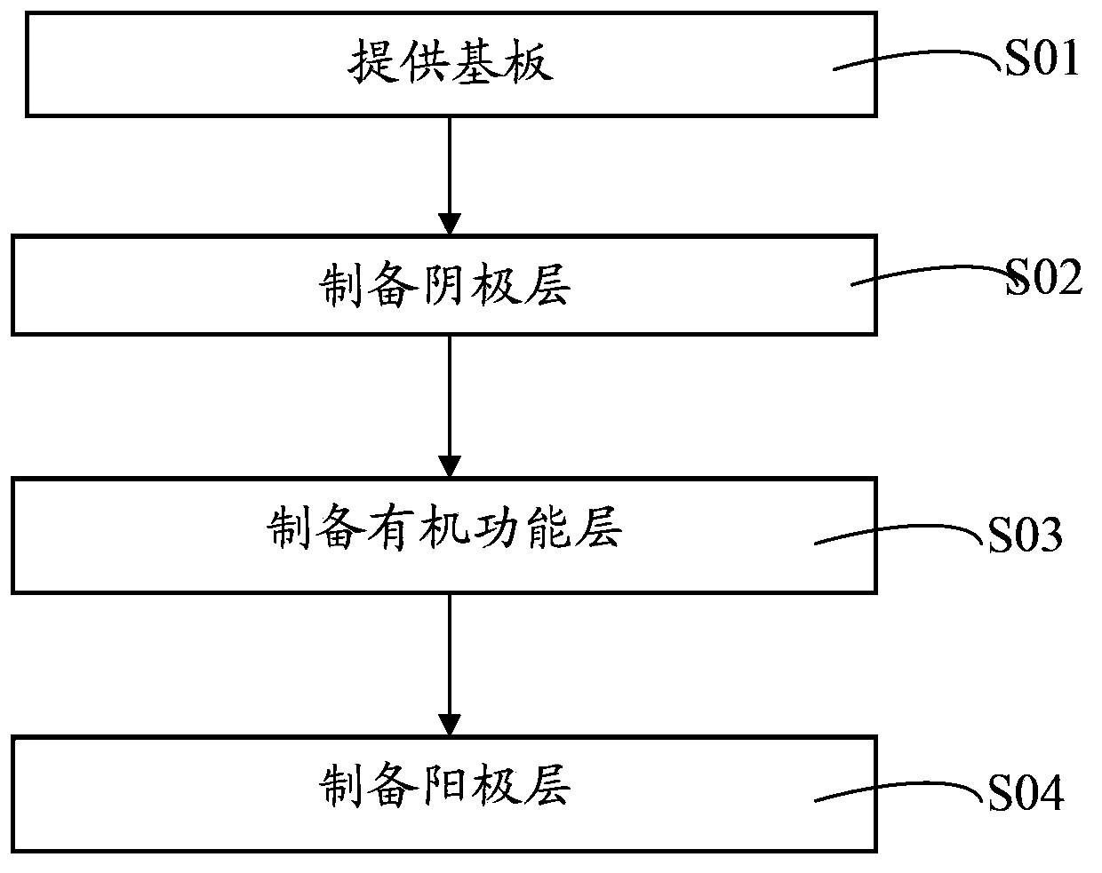
[0034] Correspondingly, the embodiment of the present invention also provides a method for preparing an inverted organic electroluminescence device as described above, the process flow of the method is as follows image 3 shown, see also Figure 1~2 . The preparation method of the inverted organic electroluminescence device comprises the following steps:

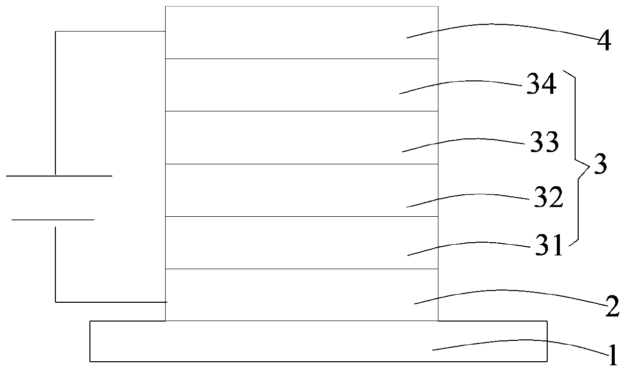
[0035] S01. Provide the substrate 1;

[0036] S02. Prepare the cathode layer 2: in a vacuum system, vapor-deposit the anode on the surface of the substrate 1 in step S01 to prepare the cathode layer 2;

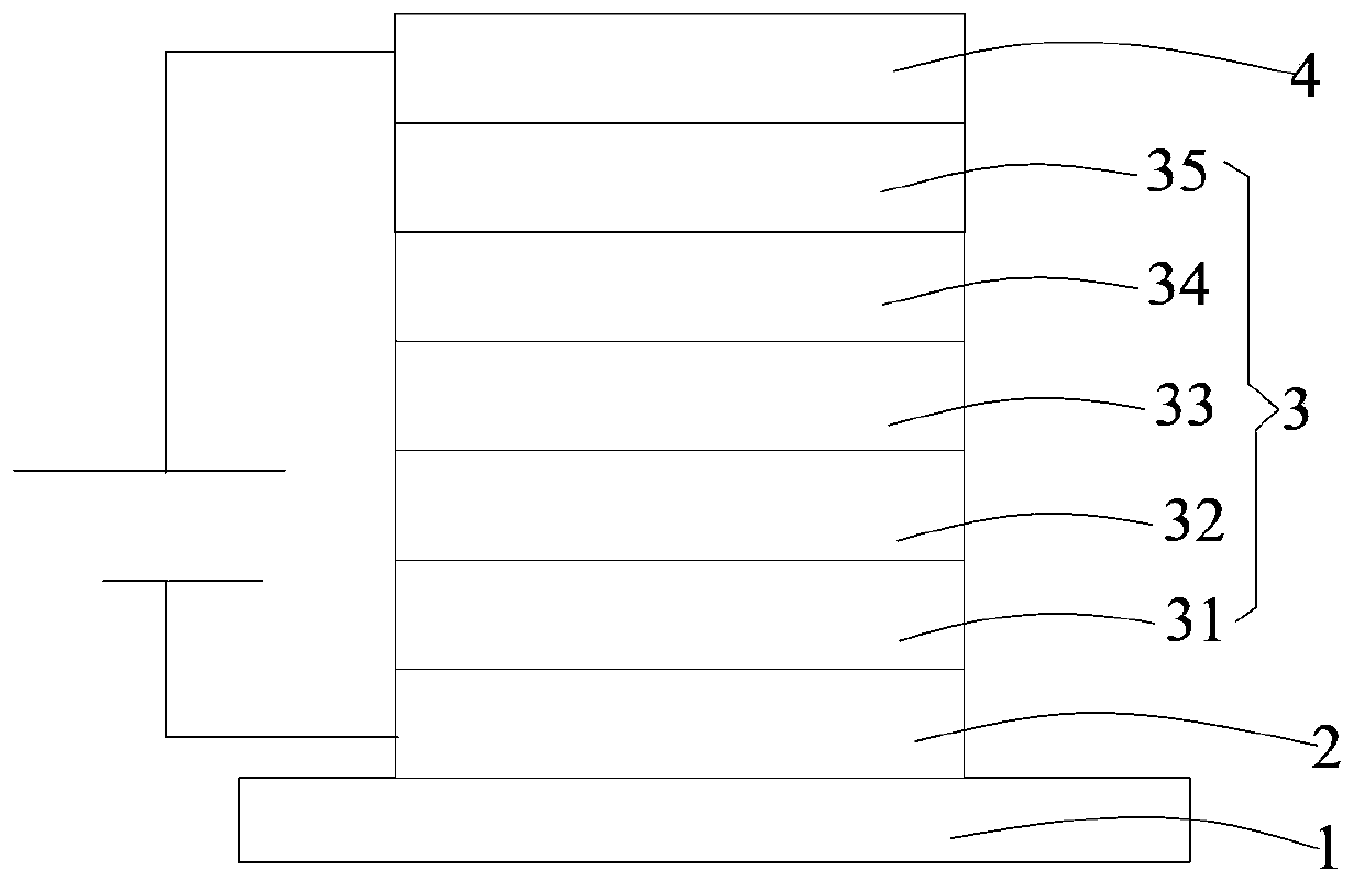
[0037] S03. Preparation of the organic functional layer 3: in a vacuum system, using an electron beam evaporation process, lanthanum hexaboride is evaporated in step S02 to prepare the surface of the cathode layer 2 opposite to the surface of the light-transmitting substrate layer 1 to form electron injection. layer 31, and then sequentially prepare an electron transport layer 32, a light emitting layer 33 and a hole tran...

Embodiment 1

[0053] An inverted organic electroluminescence device, its structure is: glass substrate / Al (20nm) / electron injection layer LaB 6 (0.5nm) / electron transport layer (TPBi, 30nm) / luminescent layer (DPVBi, 10nm) / hole transport layer (TCTA, 30nm) / hole injection layer (CuPc, 10nm) / Ag (100nm). Wherein, the size of the light-emitting area of ​​the inverted organic electroluminescence device is 3mm×3mm.

[0054] Its preparation method is as follows:

[0055] (1) At a vacuum of 10 -4 Prepared in the vacuum coating system of Pa, the glass substrate is cleaned with cleaning agent, then ultrasonically cleaned with distilled water and acetone in turn, and then in the coating system;

[0056] (2) Metal Al layers are evaporated sequentially on the substrate to form a cathode layer with a thickness of 20nm;

[0057] (3) LaB is sequentially prepared on the outer surface of the cathode layer 6 layer, TPBi layer, DPVBi layer, TCTA layer, CuPc layer, Ag layer, organic functional layer, and LaB...

Embodiment 2

[0061] An inverted organic electroluminescence device, its structure is: glass substrate / Al (20nm) / electron injection layer LaB 6 (15nm) / electron transport layer (TPBi, 30nm) / luminescent layer (DPVBi, 10nm) / hole transport layer (TCTA, 30nm) / hole injection layer (CuPc, 10nm) / Ag (100nm). Wherein, the size of the light-emitting area of ​​the inverted organic electroluminescence device is 3mm×3mm.

[0062] For the preparation method of the inverted organic electroluminescent device, refer to the preparation method of the inverted organic electroluminescent device in Example 1. Among them, the preparation of LaB 6 The working pressure of vacuum deposition film formation is 1×10 -5 Pa, the evaporation rate of lanthanum hexaboride is 1nm / s.


PUM


Abstract

The invention discloses an inverted organic light emission diode and a preparation method and application thereof. The inverted organic light emission diode comprises a substrate, a cathode layer, an organic function layer and an anode layer which are in stack combination sequentially. From the cathode layer to the anode layer, the organic function layer comprises an electron injection layer, an electron transfer layer, a light-emitting layer and a hole transfer layer which are in stack combination sequentially, wherein the electron injection layer is made of lanthanum hexaboride. The inverted organic light emission diode is small in drive current, long in service life, high in light-emitting efficiency, and wide in application range; and with the preparation method, requirements for the equipment is low, and preparation process condition is easy to control.

Description

technical field [0001] The invention belongs to the technical field of electric light sources, and in particular relates to an inverted organic electroluminescence device and its preparation method and application. Background technique [0002] Organic Light Emission Diode (hereinafter referred to as OLED) is a current-mode semiconductor light-emitting device based on organic materials. Its typical structure is to make a layer of tens of nanometers thick organic light-emitting material on the ITO glass as the light-emitting layer, and there is a metal electrode with a low work function above the light-emitting layer. [0003] The principle of OLED light emission is based on the action of an external electric field, electrons are injected from the cathode to the lowest unoccupied molecular orbital (LUMO) of organic matter, and holes are injected from the anode to the highest occupied orbital (HOMO) of organic matter. Electrons and holes meet, recombine, and form excitons in ...

Claims


Application Information

Patent Timeline
Patent Type & Authority Applications(China)
IPC IPC(8): H01L51/52H01L51/56H01L27/32
CPCH10K50/171H10K2102/00H10K2102/321H10K71/00
Inventor 周明杰冯小明黄辉王平
Owner OCEANS KING LIGHTING SCI&TECH CO LTD
Why Eureka
Try Eureka