A method for preparing vanadium dioxide film with high resistance change rate on silicon substrate

A technology based on vanadium dioxide and silicon substrates, applied in circuits, electrical components, gaseous chemical plating, etc., can solve the problems of complex epitaxy process, difficult control, buffer layer thickness, etc., achieve high film quality and reduce phase transition Relaxation time and the effect of improving the resistance change rate

Inactive Publication Date: 2016-09-07
UNIV OF ELECTRONICS SCI & TECH OF CHINA
View PDF3 Cites 0 Cited by
  • Summary
  • Abstract
  • Description
  • Claims
  • Application Information

AI Technical Summary

Problems solved by technology

However, the epitaxial process is complex and difficult to control, and the thick buffer layer is easy to introduce other effects, and the resistance change rate is not ideal, which needs to be further improved

Method used


Image

  • A method for preparing vanadium dioxide film with high resistance change rate on silicon substrate
  • A method for preparing vanadium dioxide film with high resistance change rate on silicon substrate
  • A method for preparing vanadium dioxide film with high resistance change rate on silicon substrate

Examples


Embodiment Construction

[0022] The present invention will be described in further detail below in conjunction with specific embodiments and accompanying drawings. It should be noted that the present invention is not limited to the embodiments.

[0023] A kind of VO with obvious preferred orientation and high resistivity change rate prepared on silicon substrate 2 A thin film method comprising the steps of:

[0024] Step 1. First select a double-sided polished Si substrate, and then clean the substrate. Soak the silicon substrate in self-prepared acid solution for 20 minutes to remove organic pollutants on the surface; rinse with a large amount of deionized water and then soak the silicon substrate with 25% HF solution for 10 minutes to remove the silicon oxide layer formed on the surface ; Rinse with deionized water; then ultrasonically clean with acetone for 10 minutes, then ultrasonically clean with alcohol for 10 minutes, finally clean with deionized water, and dry with nitrogen for later use.

...


PUM

PropertyMeasurementUnit
thicknessaaaaaaaaaa
thicknessaaaaaaaaaa
thicknessaaaaaaaaaa

Abstract

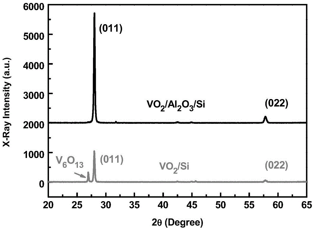
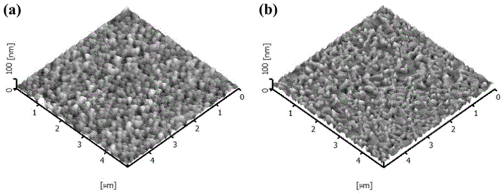
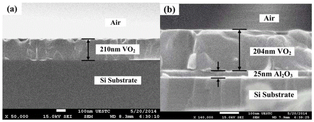
The invention provides a method for preparing a high-quality VO2 thin film on a silicon substrate, which is used for improving the resistance change rate of the VO2 thin film. The Si substrate with double-sided polishing is selected, the silicon substrate is cleaned first, and then the Al2O3 buffer layer is deposited on the Si substrate by the atomic layer deposition method. Finally, the reactive magnetron sputtering method is used to prepare the Si substrate with the Al2O3 buffer layer as the substrate. Preparation of VO2 thin films by irradiation. The process of the invention is simple and easy to realize; the prepared Si-based VO2 thin film has a strong preferred orientation, high film quality, and is closer to rutile-type VO2; through the introduction of an Al2O3 buffer layer, the phase transition relaxation time is reduced, Also greatly improved the resistance change rate, the thickness of the Al2O3 buffer layer introduced in the present invention is only 25nm, and does not cause the threshold voltage of the Si-based VO2 thin film to be too large when it is used as an electroswitch or an electric memory device; It is of great significance to promote the application of VO2 thin films in semiconductor devices.

Description

technical field [0001] The invention belongs to the technical field of functional materials and thin films, and relates to VO 2 The preparation method of the thin film is specifically a method for preparing a vanadium dioxide thin film with a high resistance change rate with obvious preferred orientation on a silicon substrate. Background technique [0002] Vanadium dioxide is a typical metal-insulator phase transition (MIT) material. At about 68 ° C, vanadium dioxide undergoes a reversible phase structure transition from monoclinic phase (M phase) to rutile phase (R phase). Accompanied by dramatic changes in optical, electrical, magnetic properties, etc. The unique phase transition properties of vanadium dioxide make it widely used in thermistor materials, photoelectric switch materials, optical storage, infrared detection materials, new semiconductor switching circuits, and terahertz modulators. Therefore, the research on vanadium dioxide thin film has very important sci...

Claims


Application Information

Patent Timeline
Patent Type & Authority Patents(China)
IPC IPC(8): C23C28/04C23C14/08C23C14/35C23C16/40
CPCH01L21/02631H01L21/02381H01L21/02565
Inventor 文岐业熊瑛陈智张怀武杨青慧田伟毛淇荆玉兰
Owner UNIV OF ELECTRONICS SCI & TECH OF CHINA
Why Eureka
Try Eureka