Double-hemisphere-structured miniature resonant gyroscope and manufacturing method thereof
A technology of resonant gyroscope and hemispherical resonator, which is applied in the field of dual-hemispherical micro-resonant gyroscope and its preparation, can solve the problem of not being able to simultaneously realize high bandwidth, high resolution, high sensitivity, high dynamic range, limiting the application range of gyroscopes, integrating / differential error and other issues, to achieve high bandwidth, high resolution, and improve the effect of measurement accuracy
- Summary
- Abstract
- Description
- Claims
- Application Information
AI Technical Summary
Problems solved by technology
Method used
Image
Examples
Embodiment 1
[0036] like figure 2 As shown, the present embodiment provides a dual hemispherical micro-resonant gyroscope, including:
[0037] a single crystal silicon substrate 1;
[0038] Sixteen evenly distributed electrodes 2;
[0039] Two symmetrical miniature hemispherical resonators 3;
[0040] A central fixed support column 4;
[0041] Wherein, the upper and lower ends of the central fixed support column 4 are respectively connected with two miniature hemispherical resonators 3, and eight electrodes 2 are evenly distributed around each miniature hemispherical resonator 3; the two miniature hemispherical resonators 3 have the same The central axes are independent of each other and do not affect each other.
[0042] In this embodiment, the material of the base 1 is monocrystalline silicon, which is directly connected to the central fixed support column 4;
[0043] In this embodiment, the material 2 of the electrodes is boron ion-doped silicon, eight of the electrodes 2 are even...
Embodiment 2
[0048] This embodiment provides a method for preparing the micro-resonant gyroscope with a dual-hemispherical structure, including the following steps:
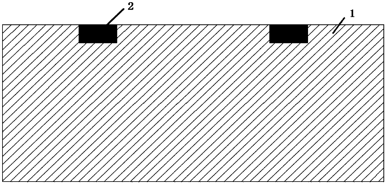
[0049] The first step, as shown in Figure 1(a), cleans the single crystal silicon substrate 1, Glue coating, photolithography, development, boron ion implantation, and glue removal processes are performed on the front side of the substrate to obtain an electrode 2 of boron ion-doped silicon material with a depth of 10 μm-50 μm on the single crystal silicon substrate 1;
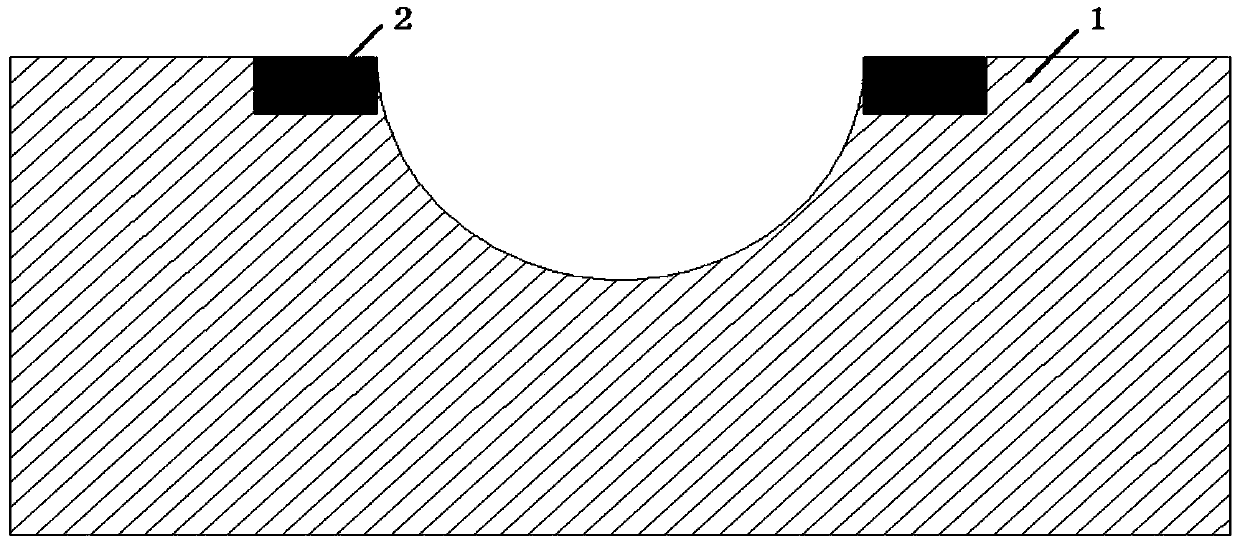
[0050] In the second step, as shown in Figure 1(b), glue coating, photolithography, development, isotropic etching, and glue removal are carried out on the basis of the first step, and a radius of 300- 700μm hemispherical deep groove;
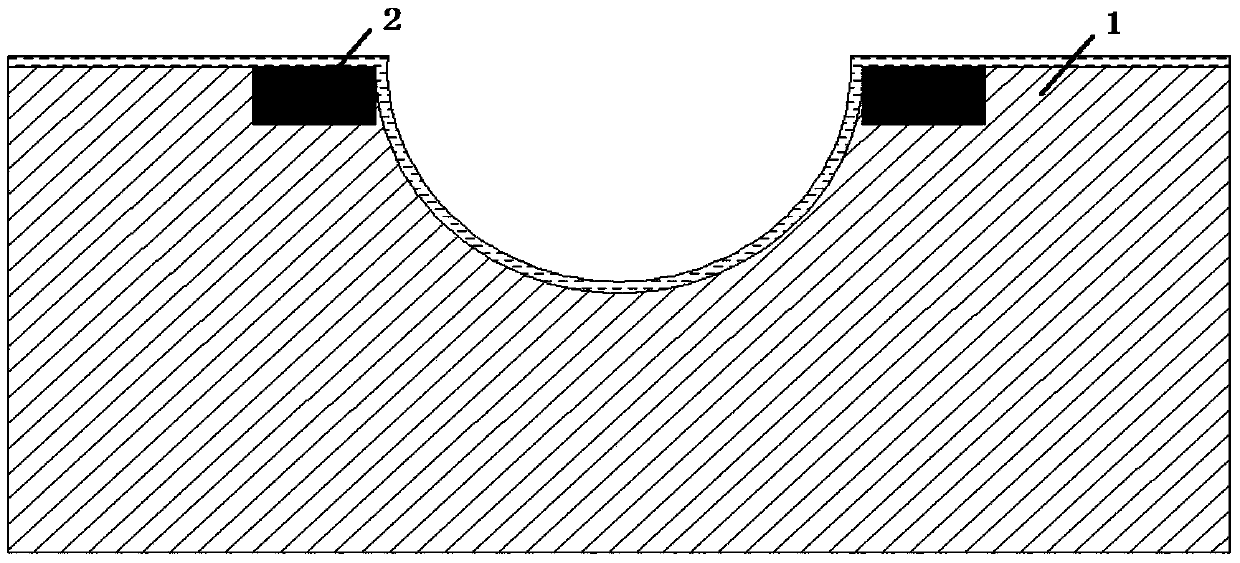
[0051] The third step, as shown in Figure 1(c), is to apply glue on the front side for protection and prepare the reverse side process;
[0052] The fourth step, as shown in Figure 1(d), repeats the first and second steps on...
PUM
| Property | Measurement | Unit |
|---|---|---|
| Depth | aaaaa | aaaaa |
| Radius | aaaaa | aaaaa |
| Thickness | aaaaa | aaaaa |
Abstract
Description
Claims
Application Information


