

Single event radiation effect resistant reinforced latch circuit
An anti-single-event radiation, latch circuit technology, applied in logic circuits, electrical components, generating electrical pulses, etc., can solve the problems of weakening anti-SEU performance, inability to shield SET, etc., to suppress SET and SEU effects, power consumption and the effect of small area overhead and improved resistance to single-event flipping effects
- Summary
- Abstract
- Description
- Claims
- Application Information
AI Technical Summary
Problems solved by technology
Method used
Image

Examples
Embodiment Construction
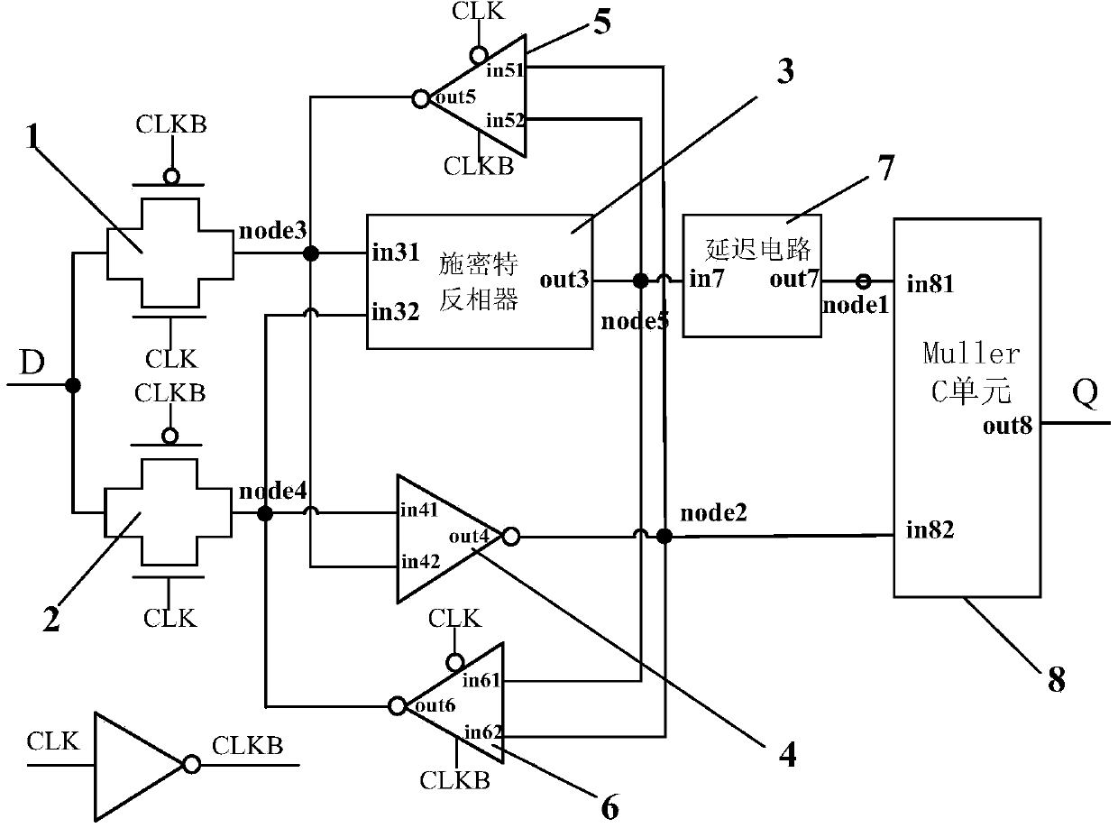
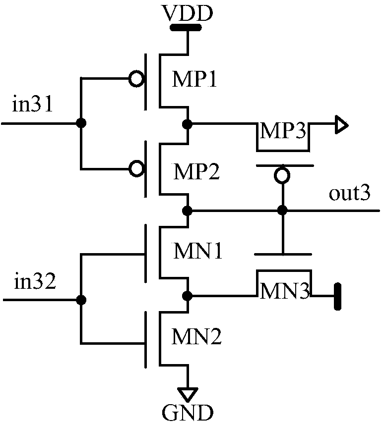
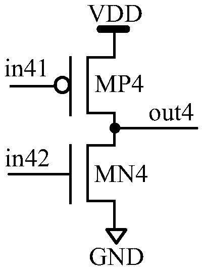
[0024] Such as figure 1 As shown, a reinforced latch circuit against single event radiation effect includes a first transmission gate unit 1, a second transmission gate unit 2, a Schmidt inverter 3, a conventional input separation inverter 4, a second transmission gate unit An input separation clocked inverter 5, a second input separation clocked inverter 6, a delay circuit 7 and a Muller C unit circuit 8, the signal input terminals of the first transmission gate unit 1 and the second transmission gate unit 2 are simultaneously connected with The data input signal D port is connected; the output of the first transmission gate unit 1 is respectively connected to the first signal input terminal in31 of the Schmidt inverter 3, the second signal input terminal in42 and the first signal input terminal of the conventional input separation inverter 4. The output terminal out5 of the input separation clocked inverter 5 is connected; the output of the second transmission gate unit 2 is...
PUM
 Abstract
Description
Claims
Application Information