Digital X-ray flat panel detector based on lead iodide photoconductive layer

A flat-panel detector and photoconductive layer technology, applied in the direction of semiconductor devices, circuits, electrical components, etc., can solve the problems of device failure, increase X-ray dose, and increase radiation absorption of patients, so as to reduce manufacturing and production costs, High blocking and absorption efficiency, effect of ensuring spatial resolution

Inactive Publication Date: 2014-12-17
朱 兴华 +1
View PDF7 Cites 18 Cited by
  • Summary
  • Abstract
  • Description
  • Claims
  • Application Information

AI Technical Summary

Problems solved by technology

[0003] Amorphous selenium materials have a low absorption rate of X-rays, and the image quality under low-dose conditions cannot be well guaranteed. Increasing the X-ray dose will not only increase the patient's radiation absorption, but also have higher requirements for the X-ray system. , it is also easy to cause the aging failure of the material
More importantly, digital X-ray flat-panel detectors based on amorphous selenium have strict requirements on the use environment, and local crystallization of amorphous selenium materials will occur in a certain range above room temperature, thereby losing the photoelectric conversion function and causing device failure.

Method used


Image

  • Digital X-ray flat panel detector based on lead iodide photoconductive layer
  • Digital X-ray flat panel detector based on lead iodide photoconductive layer

Examples


Embodiment Construction

[0018] In order to make the technical problems, technical solutions and advantages to be solved by the embodiments of the present invention clearer, further description will be made below in conjunction with the accompanying drawings and specific embodiments, which should not be construed as limiting the scope of protection of the present invention. Those skilled in the art Some non-essential improvements and adjustments can be made according to the content of the present invention above, but this still belongs to the protection scope of the present invention.

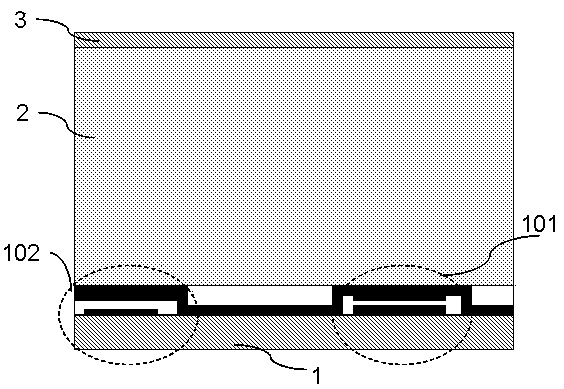
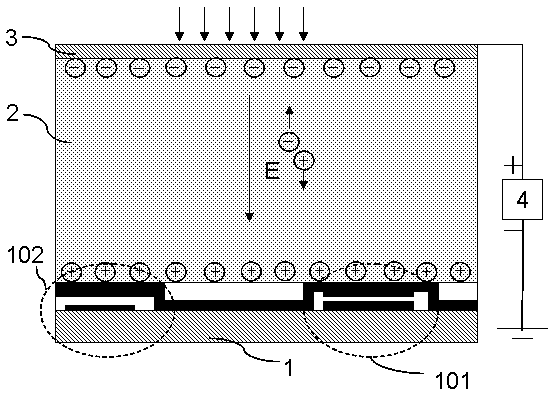
[0019] see figure 1 , is a cross-sectional view of the digital X-ray flat panel detector based on the lead iodide photoconductive layer of the present invention. The structure of the digital X-ray flat panel detector is as follows figure 1 As shown, it includes: a matrix type thin film transistor glass substrate 1, which is used to read out charge signals. According to the application field, the area size of the matri...


PUM


Abstract

The invention relates to a digital X-ray flat panel detector based on a lead iodide photoconductive layer. The detector comprises a matrix thin film transistor glass substrate, the photoconductive layer and a top electrode layer, wherein the photoconductive layer is disposed on the matrix thin film transistor glass substrate and the top electrode layer is disposed on the surface of the photoconductive layer. The digital X-ray flat panel detector has the advantages that a lead iodide material layer is used as the photoconductive layer, X-ray photons are directly converted into charge signals to achieve digital X-ray imaging, the lead iodide material layer is good in structure and performance and simple in preparation process, and low-cost, large-area, continuous and stable preparation with large-thickness requirements can be achieved easily; radiation medical imaging cost and non-destructive detection imaging cost can be lowered, and the detector can be popularized in the fields of radiation imaging.

Description

technical field [0001] The invention relates to a digital X-ray flat-panel imaging device, in particular to a lead iodide photoconductive layer-based digital X-ray flat-panel detector for radiological medical imaging and non-destructive detection imaging, belonging to the field of radiation detection and imaging. Background technique [0002] At present, digital X-ray imaging equipment mainly has two types of flat panel detectors. An indirect conversion amorphous silicon (a-Si) digital X-ray flat panel detector, using a scintillator (cesium iodide CsI) or a phosphor layer (gadolinium oxysulfide GdSO) plus an amorphous silicon photodiode plus electrons The structure of switching thin film transistors (Thin film Transtors, TFT). The other is a direct-conversion amorphous selenium (a-Se) digital X-ray flat panel detector. The amorphous selenium photoconductive layer is prepared on an arrayed thin film transistor glass substrate to form an amorphous selenium plus TFT detector s...

Claims


Application Information

Patent Timeline
Patent Type & Authority Applications(China)
IPC IPC(8): H01L27/146H01L31/032
Inventor 朱兴华孙辉
Owner 朱 兴华
Why Eureka
Try Eureka