Focus detection method based on grating Talbot effect

A technology of Taber and focus detection, which is applied in optics, optical components, and optical devices, etc., can solve the problems of inability to take into account focus detection accuracy and efficiency, low system anti-interference ability, etc., and achieve high engineering practicability and high anti-interference ability. Ability, the effect of high focus detection accuracy

Inactive Publication Date: 2014-12-24
INST OF OPTICS & ELECTRONICS - CHINESE ACAD OF SCI
View PDF4 Cites 10 Cited by
  • Summary
  • Abstract
  • Description
  • Claims
  • Application Information

AI Technical Summary

Problems solved by technology

[0007] Generally speaking, the currently reported focus detection methods have low syste...

Method used


Image

  • Focus detection method based on grating Talbot effect
  • Focus detection method based on grating Talbot effect
  • Focus detection method based on grating Talbot effect

Examples


Embodiment Construction

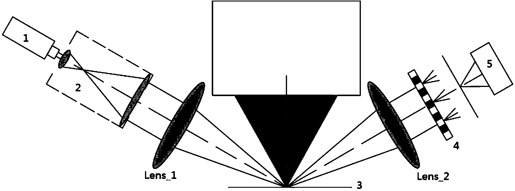
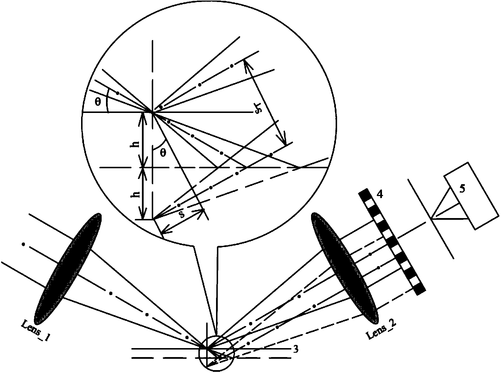
[0020] In order to realize the on-line precision focus measurement of silicon wafers in the lithography system, this project is based on the Talbot effect of gratings. By analyzing the phase distribution of the interference fringes of the Talbot effect, the high-precision focus measurement of silicon wafers is completed. The focus detection system is as follows: figure 1 shown.

[0021] The focus detection method based on the grating Taber effect and applied to high-precision photolithography machines according to the present invention is characterized in that: the detection system is a 4f optical system consisting of a light source 1, a beam collimation and beam expansion system 2, and lens groups Lens_1 and Lens_2. system, tested silicon wafer 3, diffraction grating 4 and CCD detector 5. 4f optical system composed of lens groups Lens_1 and Lens_2: when the tested silicon wafer 3 is located on the confocal plane of the 4f system, the outgoing plane wavefront of the collimated...


PUM


Abstract

The invention relates to a focus detection method based on a grating Talbot effect. The method is used for detecting the position of a silicon chip of a photoetching machine system in real time to complete the high-accuracy leveling and focusing of the silicon chip. By virtue of a detection system, the high-accuracy focus detection of the silicon chip of a photoetching machine is completed according to the self-imaging phase change of the grating Talbot effect due to the fact that the silicon chip is out of focus. When the silicon chip is positioned on a focal plane, grating forming wave-front is planar wave-front. When the silicon chip is out of focus, the imaging wave-front is spherical wave-front. The focus detection method is higher in anti-interference capacity and better in technological adaptability.

Description

technical field [0001] The invention relates to a focusing method based on the grating Taber effect, which is used for high-precision leveling and focusing of silicon wafers of photolithography machines, and belongs to the field of microelectronic equipment and microprocessing. Background technique [0002] Microelectronics technology with large-scale integrated circuits as the core develops rapidly in accordance with the development law of "one-generation technology, one-generation equipment, and one-generation devices". With the emergence of nano-devices, new requirements are put forward for micro-fabrication and micro-nano detection technology. Optical projection lithography technology uses the principle of optical projection to transfer the high-resolution pattern on the reticle to the silicon wafer through the projection objective lens. Because the optical projection lithography technology can not only have the high resolution of contact lithography, but also avoid dama...

Claims


Application Information

Patent Timeline
IPC IPC(8): G03F7/20G03F9/00
CPCG03F9/7026G01B9/02097G02B7/28
Inventor 朱咸昌胡松赵立新
Owner INST OF OPTICS & ELECTRONICS - CHINESE ACAD OF SCI
Why Eureka
Try Eureka