Preparation method of dual contact hole etching stop layer

An etching stop layer, double contact technology, applied in semiconductor/solid-state device manufacturing, electrical components, circuits, etc., can solve the problems of increasing process cost and process complexity, avoiding negative effects, avoiding complexity, and improving device power. performance effect

Inactive Publication Date: 2014-12-24
SHANGHAI HUALI MICROELECTRONICS CORP
View PDF5 Cites 4 Cited by
  • Summary
  • Abstract
  • Description
  • Claims
  • Application Information

AI Technical Summary

Problems solved by technology

Since two-step photolithography is required in the traditional Dual CESL process to remove high-tensile-stress silicon nitride in the PM

Method used


Image

  • Preparation method of dual contact hole etching stop layer
  • Preparation method of dual contact hole etching stop layer
  • Preparation method of dual contact hole etching stop layer

Examples


Embodiment Construction

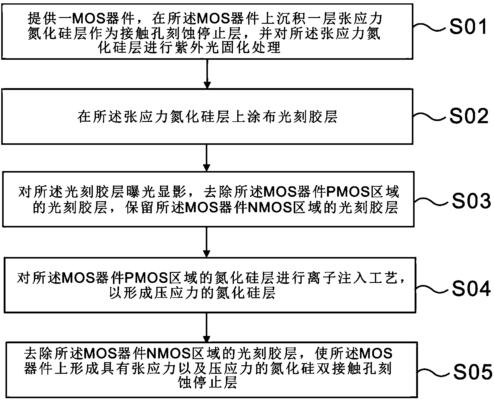
[0026] In order to make the content of the present invention clearer and easier to understand, the content of the present invention will be further described below in conjunction with the accompanying drawings. Of course, the present invention is not limited to this specific embodiment, and general replacements known to those skilled in the art are also covered within the protection scope of the present invention. Secondly, the present invention is described in detail by means of schematic diagrams. When describing the examples of the present invention in detail, for the convenience of explanation, the schematic diagrams are not partially enlarged according to the general scale, which should not be used as a limitation of the present invention.

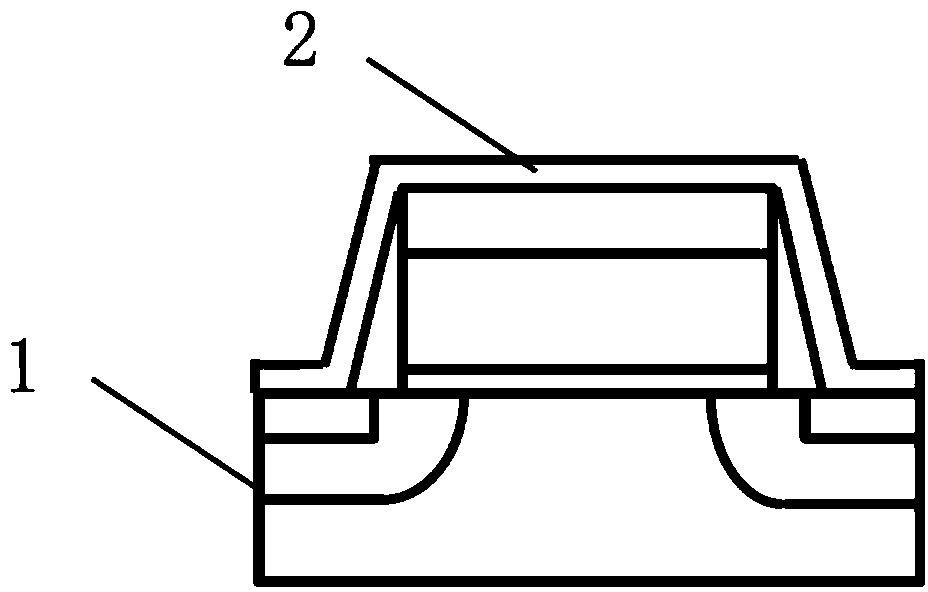
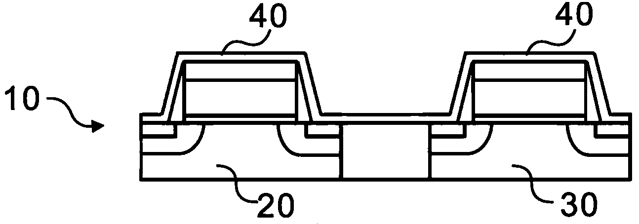
[0027] It should be noted that, in the following examples, using Figure 3 ~ Figure 7 The schematic diagram in the figure describes in detail the device structure formed according to the method for manufacturing the etching stop layer...


PUM

PropertyMeasurementUnit
Wavelengthaaaaaaaaaa

Abstract

The invention provides a preparation method of a dual contact hole etching stop layer. The preparation method comprises the steps of 01, providing an MOS device, depositing a tensile stress silicon nitride layer on the MOS device as a contact hole etching stop layer and carrying out ultraviolet light polymerization treatment on the tensile stress silicon nitride layer; 02, coating the tensile stress silicon nitride layer with a photoresist layer; 03, carrying out exposure and development on the photoresist layer, removing the part, in the PMOS area of the MOS device, of the photoresist layer and retaining the part, in the NMOS area of the MOS device, of the photoresist layer; 04, carrying out ion implantation on the part, in the PMOS area of the MOS device, of the silicon nitride layer to form a pressure stress silicon nitride layer; 05, removing the part, in the NMOS area of the MOS device, of the photoresist layer. Compared with a traditional preparation process for the dual contact hole etching stop layer, the preparation method is simpler and lower in cost, thereby having the significant advancement of improving the device performance at a low cost.

Description

technical field [0001] The invention relates to the technical field of semiconductor integrated circuit manufacturing, and more specifically, to a preparation method of an etching stop layer for double contact holes based on strained silicon technology. Background technique [0002] With the development of CMOS integrated circuit manufacturing process and the reduction of critical dimensions, many new methods have been applied to device manufacturing process to improve device performance. The high-stress silicon nitride film is introduced into the integrated circuit manufacturing process because it can effectively improve the carrier mobility of the MOS tube, thereby increasing the operating speed of the device. The compressive stress in the direction of the PMOS channel can improve the hole mobility in the PMOS device, and the tensile stress in the direction of the NMOS channel can improve the electron mobility in the NMOS device. [0003] see figure 1 , figure 1 It is a...

Claims


Application Information

Patent Timeline
IPC IPC(8): H01L21/318
CPCH01L21/76831
Inventor 雷通邱裕明
Owner SHANGHAI HUALI MICROELECTRONICS CORP
Why Eureka
Try Eureka