Front metal process for compression joint IGBT
A metal technology, crimping technology, applied in the direction of electrical components, electrical solid devices, semiconductor/solid device manufacturing, etc.
- Summary
- Abstract
- Description
- Claims
- Application Information
AI Technical Summary
Problems solved by technology
Method used
Image
Examples
Embodiment Construction
[0030] The present invention will be further described below in conjunction with specific embodiment and accompanying drawing, set forth more details in the following description so as to fully understand the present invention, but the present invention can be implemented in many other modes different from this description obviously, Those skilled in the art can make similar promotions and deductions based on actual application situations without violating the connotation of the present invention, so the content of this specific embodiment should not limit the protection scope of the present invention.
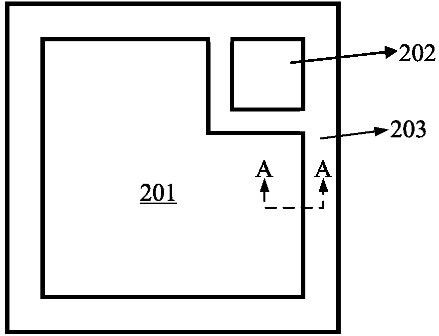
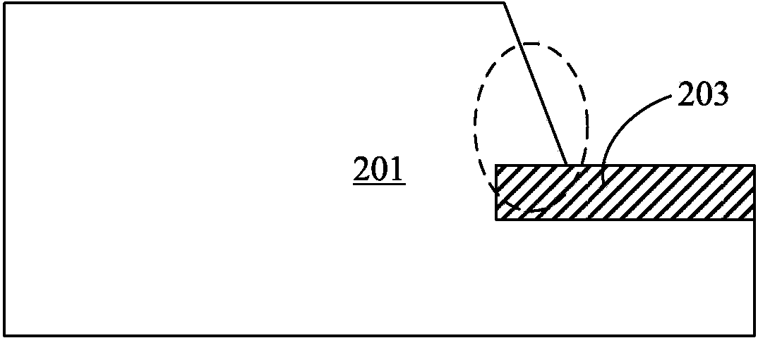
[0031] In order to illustrate the technical solution of the present invention more clearly, here is a preliminary introduction to the structure of the front metal layer of the pressure-contact IGBT. figure 1 A schematic diagram of the plane position of the emitter pad and the gate pad of the pressure-connected IGBT realized by the front metal process of an embodiment of the pre...
PUM
| Property | Measurement | Unit |
|---|---|---|
| Bottom width | aaaaa | aaaaa |
| Thickness | aaaaa | aaaaa |
| Second thickness | aaaaa | aaaaa |
Abstract
Description
Claims
Application Information


