

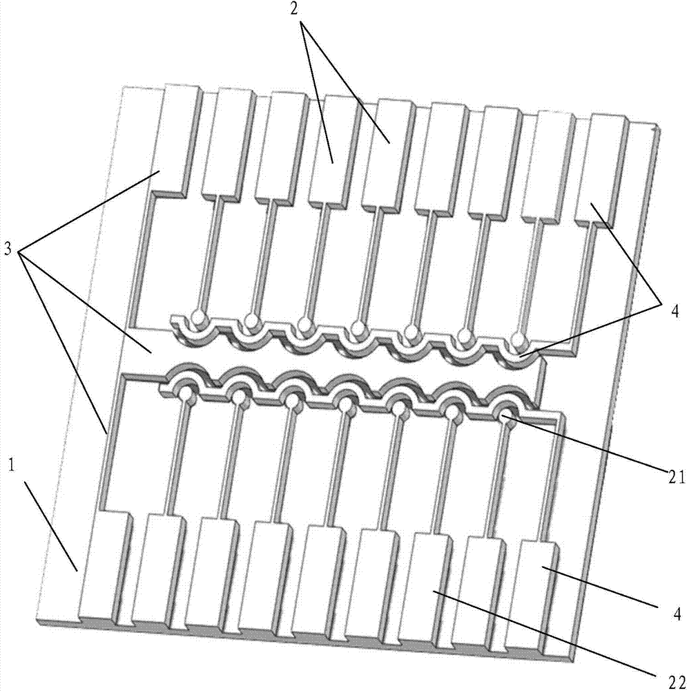
Dual-detection biosensing chip and preparation method thereof and DNA detection method
A biosensing and dual-detection technology, applied in the field of bioelectronics, electrochemistry and optical sensing, can solve the problems of time-consuming, cumbersome process and high cost, and achieve the effects of reducing false positives, accurate detection results and short time-consuming
- Summary
- Abstract
- Description
- Claims
- Application Information
AI Technical Summary
Problems solved by technology
Method used
Image

Examples
preparation example Construction
[0035] The present invention further proposes the preparation method of the above-mentioned dual detection biosensor chip, comprising the following steps:
[0036] S10, preparing a nano-gold electrode;
[0037] S20, assembling a dual-detection biosensor chip;
[0038] S30, immobilizing the DNA probe on the nano-gold electrode;
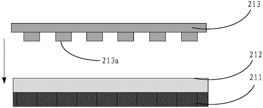
[0039] Among the above-mentioned steps of the present invention, step S10 is to prepare a nano-gold electrode, and the following steps can be used in its specific implementation. For details, see Figure 2-7 The schematic diagram shown:
[0040] S11, obtaining an ITO glass 211, and cleaning and drying the surface thereof for use;
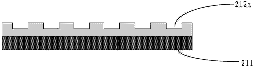
[0041] S12, coating a resist layer 212 on the surface of the ITO glass 211;
[0042] S13, generating nanoscale-sized grooves 214 on the surface of the resist layer 212;
[0043] S14, depositing a protective layer 215 on the non-groove surface of the resist layer 212;
Embodiment 1
[0070] S11, choose an ITO circular glass substrate with a thickness of 1 mm and a diameter of 1 cm, ultrasonically clean it with ammonia water, ethanol and distilled water for 3 minutes, and dry it with nitrogen;
[0071] In this step, the ITO glass substrate is selected as a circular shape for the convenience of electrode assembly and electrode preparation; of course, it can also be replaced with other regular or irregular shapes according to the needs, not limited to the circle shaped shape.
[0072] S12, coating a single-layer imprinting resist such as resin etc. on the ITO circular glass substrate cleaned in step S11, forming a resin layer on the ITO circular glass substrate;
[0073] S13, obtain an embossing plate, the embossing surface of the embossing plate has a nanoscale convex model; after the embossing surface of the embossing plate is pressed against the resin layer and the ITO circular glass substrate, the embossing plate is removed , then a groove matching the c...
PUM
| Property | Measurement | Unit |
|---|---|---|
| size | aaaaa | aaaaa |
| diameter | aaaaa | aaaaa |
Abstract
Description
Claims
Application Information