Etching method for III-V-group compound semiconductor materials

A III-V and compound technology, applied in the field of etching of III-V compound semiconductor materials, can solve the problems of poor surface morphology, poor etching precision, and reduced material properties, so as to achieve low surface damage and improve lines Accuracy, the effect of reducing the processing line width

Inactive Publication Date: 2015-01-14
UNIV OF ELECTRONICS SCI & TECH OF CHINA
View PDF4 Cites 11 Cited by
  • Summary
  • Abstract
  • Description
  • Claims
  • Application Information

AI Technical Summary

Problems solved by technology

[0005] The invention provides an etching method for III-V compound semiconductor materials, which can overcome the poor surface morphology, lattice damage, poor etching precision and material properties caused by high temperature oxidation caused by ordinary dry etching It has the characteristics of precise controllable etching depth and almost no damage to III-V compound semiconductor materials.

Method used


Image

  • Etching method for III-V-group compound semiconductor materials
  • Etching method for III-V-group compound semiconductor materials
  • Etching method for III-V-group compound semiconductor materials

Examples


Embodiment Construction

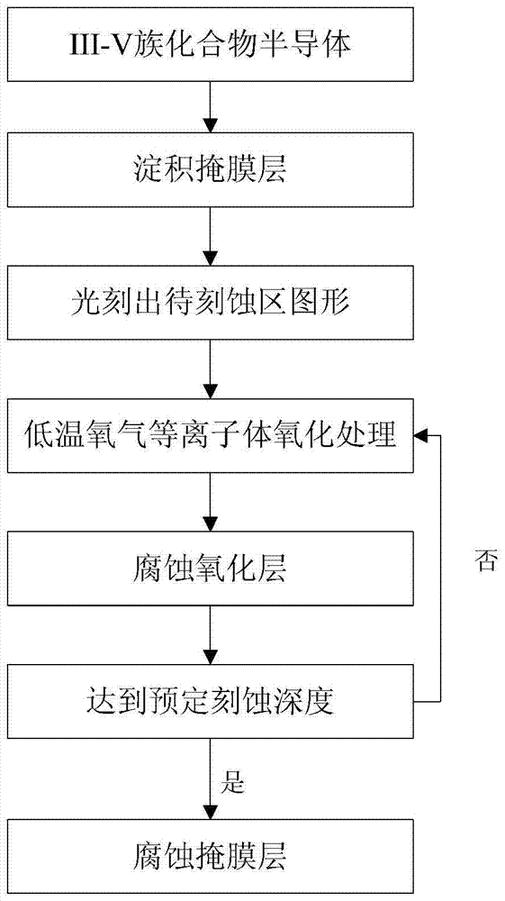
[0026] The etching method of the III-V group compound semiconductor material of the present invention will be described in detail below through specific examples and accompanying drawings.

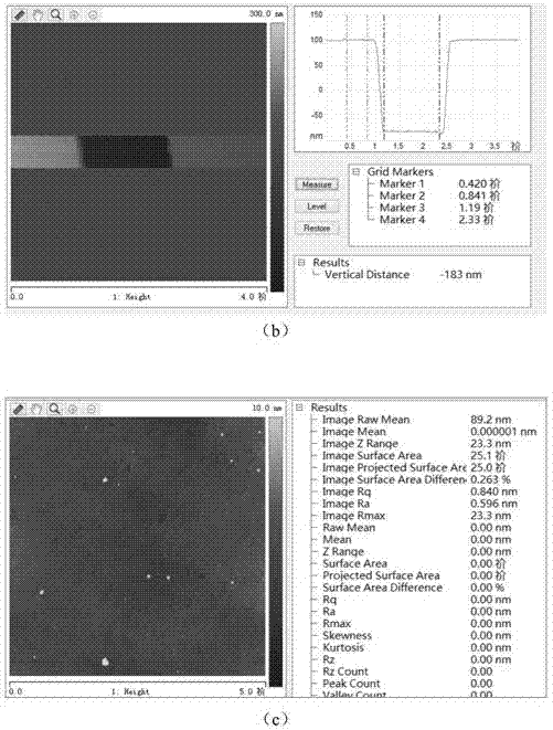
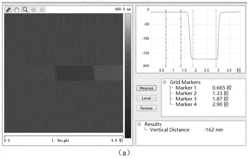
[0027] Taking the AlGaN / GaN heterojunction material as an example, the principle of the present invention to oxidize and wet-etch gallium nitride-based wafers is to perform oxygen plasma treatment on the surface of the AlGaN barrier layer under low temperature conditions, and The surface not protected by Si3N4 will be oxidized by oxygen plasma in AlGaN to form Al X o Y and Ga X o Y And nitrogen oxides, the acidic solution will dissolve the oxide layer without affecting AlGaN, forming a corrosion groove.

[0028] Taking AlGaN / GaN HEMT groove gate etching process as an example, the method will be described in detail below. The gallium nitride-based material groove etching steps include:

[0029] A Si3N4 mask layer with a thickness of 160nm was prepared on the surface of the GaN wafer by ...


PUM

PropertyMeasurementUnit
thicknessaaaaaaaaaa
surface roughnessaaaaaaaaaa

Abstract

The invention provides an etching method for III-V-group compound semiconductor materials and belongs to the technical field of semiconductor technologies. According to the etching method, the dry oxidation technology with low-temperature oxygen plasma oxidization and the technology for wet etching of an oxidation layer are combined to be used for etching of the III-V-group compound semiconductor materials, the etching depth can be accurately controlled, wherein the etching precision can reach a high level, please see the level in the specification. The etching method for the III-V-group compound semiconductor materials has the advantages that the surface damage is low, the surface appearance is good, the precision of lines of etched grating grooves can be improved, and the width of a processing line can be reduced. Oxygen plasma treatment is conducted on the surface of a wafer at a low temperature, and therefore current reduction due to heterojunction relaxation which is possibly caused by high-temperature oxidation can be effectively avoided. The etching method can be widely used for etching of shallow slots or fine lines of the III-V-group compound semiconductor materials, such as etching of an ohmic contact groove of a gallium-nitride-based device or groove grid of an enhancement device.

Description

technical field [0001] The invention belongs to the technical field of semiconductor technology and relates to an etching method for III-V group compound semiconductor materials. technical background [0002] The III-V compound semiconductor gallium nitride (GaN) and gallium arsenide (GaAs), as a typical representative of compound semiconductors, have many excellent characteristics. Gallium nitride and gallium arsenide materials have high electron mobility and high two-dimensional electron gas (2DEG) concentration, and have been developed rapidly in the past ten years. Gallium nitride (GaN) materials have stable chemical properties, high temperature resistance, and corrosion resistance, and have inherent advantages in high-frequency, high-power, and radiation-resistant applications. Gallium arsenide (GaAs) material is an excellent channel material and has broad prospects in future CMOS applications. [0003] Recessed gate etching of high-performance enhanced GaN-based devi...

Claims


Application Information

Patent Timeline
Patent Type & Authority Applications(China)
IPC IPC(8): H01L21/3065H01L21/308
CPCH01L21/3065H01L21/308
Inventor 周琦牟靖宇鲍旭汪玲施媛媛靳旸陈博文陈万军张波
Owner UNIV OF ELECTRONICS SCI & TECH OF CHINA
Why Eureka
Try Eureka