Method for manufacturing silicon carbide semiconductor device

A manufacturing method and semiconductor technology, applied in the fields of semiconductor/solid-state device manufacturing, semiconductor devices, electrical components, etc., can solve the problems of poor target use efficiency, poor film thickness uniformity, and short target life, so as to suppress excess Residue, improve the efficiency of use, the effect of uniform film thickness

Inactive Publication Date: 2015-01-21
FUJI ELECTRIC CO LTD
View PDF7 Cites 1 Cited by
  • Summary
  • Abstract
  • Description
  • Claims
  • Application Information

AI Technical Summary

Problems solved by technology

In the magnetron sputtering method generally used to form a metal film, it is known that by repeatedly forming a ferromagnetic nickel film, the leakage magnetic field lines at the outer periphery of the target are reduced, and erosion is concentrated in the center of the target, resulting in a uniform film thickness. Sexual deterioration
In addition, since the deposition speed decreases at the outer periphery of the target, and on the other hand, the deposition speed increases toward the center of the target, so the life of the target is shortened, and the use efficiency of the target is deteriorated.

Method used


Image

  • Method for manufacturing silicon carbide semiconductor device
  • Method for manufacturing silicon carbide semiconductor device
  • Method for manufacturing silicon carbide semiconductor device

Examples


Embodiment approach

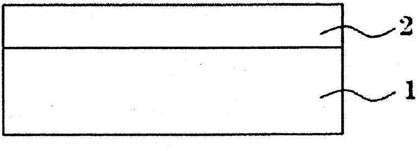
[0032] A method of manufacturing a silicon carbide Schottky barrier diode is illustrated as an example, and a method of manufacturing a silicon carbide semiconductor device according to an embodiment of the present invention will be described in detail below.

[0033] Figure 1~6 It is a cross-sectional schematic diagram for explaining the manufacturing process of the silicon carbide Schottky barrier diode concerning embodiment of this invention. First, if figure 1 As shown, the preparation is doped with e.g. 1 x 10 18 cm -3 A high-concentration n-type silicon carbide substrate 1 having a (0001) plane with a nitrogen thickness of 350 μm. Next, doped, for example, 1.8×10 16 cm -3 A low-concentration n-type silicon carbide drift layer 2 of nitrogen with a thickness of 6 μm.

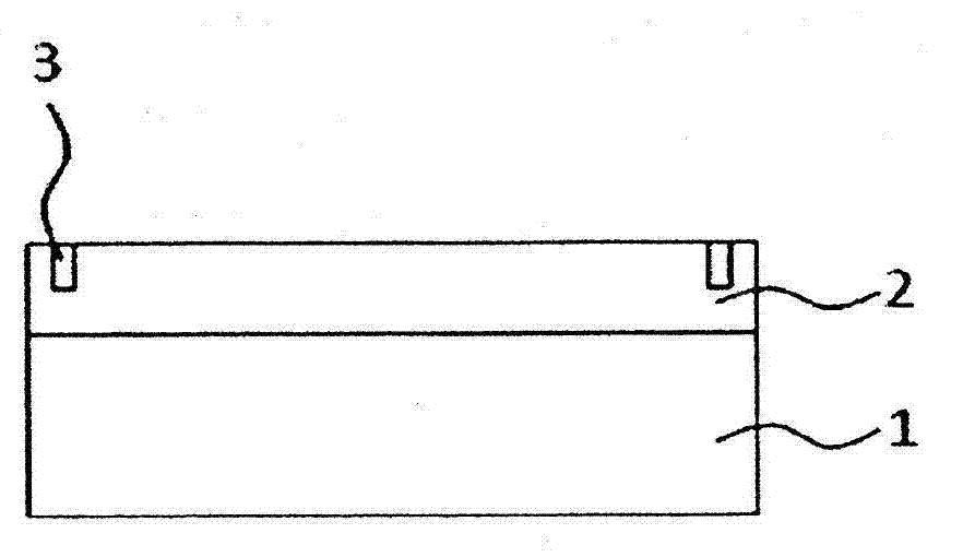
[0034] Next, if figure 2 As shown, in order to form an n-type region 3 for a channel stopper (channel stopper), for example, phosphorus (P) is implanted into the low-concentration n-type silicon car...


PUM


Abstract

An ohmic electrode (6) of a silicon carbide semiconductor device is produced by forming an ohmic metal film on a silicon carbide substrate (1) by sputtering a target that is formed of a mixture or alloy in which nickel and a metal that reduces the magnetic permeability of nickel and forms a carbide are adjusted to a predetermined composition ratio, and firing the ohmic metal foil by a heat treatment. Consequently, there can be produced an ohmic electrode (6) of a silicon carbide semiconductor device, said ohmic electrode (6) having a uniform thickness and being free from separation, while improving the efficiency of the target.

Description

technical field [0001] The present invention relates to a method for manufacturing a silicon carbide semiconductor device, in particular to a method for manufacturing an ohmic electrode of a silicon carbide semiconductor device. Background technique [0002] In the past, for the purpose of high-frequency and high-power control, the performance of power devices using silicon (Si) substrates (hereinafter referred to as silicon power devices) has progressed. However, since silicon power devices cannot be used at high temperatures, the use of new semiconductor materials has been studied in response to demands for higher performance power devices. [0003] Since silicon carbide (SiC) has a wide bandgap about three times that of silicon, it has excellent controllability of electrical conductivity at high temperatures, and since it has an insulation breakdown voltage about one order of magnitude higher than that of silicon, it can be used as a high withstand voltage Substrate mate...

Claims


Application Information

Patent Timeline
Patent Type & Authority Applications(China)
IPC IPC(8): H01L21/28H01L21/285H01L21/336H01L29/12H01L29/78
CPCH01L29/6606H01L29/401H01L29/0619H01L29/872H01L21/0485H01L29/1608H01L29/0638H01L21/02529H01L21/02636H01L21/285H01L21/2855H01L29/66143
Inventor 吕民雅仲俣伸一木下明将福田宪司
Owner FUJI ELECTRIC CO LTD
Why Eureka
Try Eureka