Semiconductor device formation method

A semiconductor and device technology, applied in the field of semiconductor device formation, can solve problems such as poor performance of NMOS metal transistors, and achieve the effect of improving performance and improving performance.

Active Publication Date: 2015-02-11
SEMICON MFG INT (SHANGHAI) CORP
View PDF8 Cites 3 Cited by
  • Summary
  • Abstract
  • Description
  • Claims
  • Application Information

AI Technical Summary

Problems solved by technology

[0008] The problem solved by the present invention is the process of simultaneously forming PMOS metal transistors and NMOS metal transistors on the same substrate, and the formed NMOS metal transistors have poor performance

Method used


Image

  • Semiconductor device formation method
  • Semiconductor device formation method
  • Semiconductor device formation method

Examples


no. 1 example

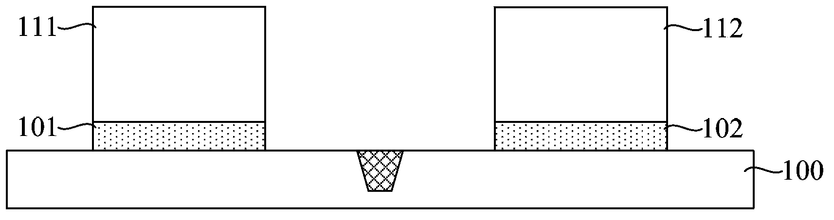
[0048] refer to Figure 4 , providing a substrate 300, the substrate 300 includes a first active region I and a second active region II, the types of the first active region I and the second active region II are opposite.

[0049] In this embodiment, the first active region I is a P-type active region, the second active region II is an N-type active region, and the first active region I and the second active region II are shallow trench isolation structure (not numbered). A PMOS transistor is formed in the first active region I, and an NMOS transistor is formed in the second active region II.

[0050] In this embodiment, the substrate 300 is a silicon substrate, a germanium substrate, or a silicon-on-insulator substrate, etc.; or it may also include other materials, such as III-V group compounds such as gallium arsenide. Those skilled in the art can select the substrate according to the type of transistors formed on the substrate 300 , so the type of the substrate should not l...

no. 2 example

[0087] The difference between the second embodiment and the first embodiment is that after the interlayer dielectric layer is formed, the second dummy gate is removed to form a second dummy gate trench, and a second dummy gate trench is formed on the bottom and side walls of the second dummy gate trench. a third gate dielectric layer;

[0088] After forming the third gate dielectric layer, the first dummy gate is removed to form a first dummy gate trench.

[0089] In another embodiment, it may also be: removing the second dummy gate structure to form a second dummy gate trench;

[0090] After forming the second dummy gate trench, removing the first dummy gate to form the first dummy gate trench;

[0091] Afterwards, a third gate dielectric layer is formed on the sidewall and bottom of the second dummy gate trench.

[0092] Wherein, parameters such as the thickness of the first gate dielectric layer and the third gate dielectric layer, and the mass concentration of chromium c...


PUM


Abstract

The invention relates to a semiconductor device formation method. The semiconductor device formation method comprises steps that a substrate is provided, the substrate has a first active region and a second active region, and the first active region and the second active region have opposite types; a first dummy grid electrode structure at the first active region and a second dummy grid electrode structure at the second active region are formed on the substrate, the first dummy grid electrode structure comprises a first grid medium layer and a first dummy grid electrode, and the second dummy grid electrode structure comprises a second grid medium layer and a second dummy grid electrode; an interlayer dielectric layer is formed on the substrate, and the upper surface of the interlayer dielectric layer is level with the upper surface of the first dummy grid electrode and the upper surface of the second dummy grid electrode; the first dummy grid electrode is removed to form a first dummy grid slot; the second dummy grid electrode is removed to form a second dummy grid slot; third grid dielectric layers are formed at the bottom portion and side walls of the second dummy grid slot. According to the semiconductor device formation method, parameters of material composition and thickness of the first grid dielectric layer and the third grid dielectric layers can be respectively adjusted, and thereby performance of transistors of the corresponding first grid dielectric layer and the third grid dielectric layers is improved.

Description

technical field [0001] The invention relates to the technical field of semiconductors, in particular to a method for forming a semiconductor device. Background technique [0002] In the prior art, metal gate transistors using a high-K gate dielectric layer are generally accepted. Compared with traditional CMOS transistors, metal transistors using high-K gate dielectric layers can reduce gate leakage current, improve time-dependent dielectric breakdown (Time Dependent Dielectric Breakdown, TDDB) performance, and reduce the probability of gate dielectric layer breakdown. possibility. [0003] Figure 1 ~ Figure 3 It is a schematic cross-sectional structure diagram of a method for simultaneously forming a PMOS metal transistor and an NMOS metal transistor on the same substrate in the prior art. [0004] refer to figure 1 , the substrate 100 includes a P-type active region and an N-type active region, and a first high-K gate dielectric layer 101 and a first dummy gate locate...

Claims


Application Information

Patent Timeline
Patent Type & Authority Applications(China)
IPC IPC(8): H01L21/8238H01L21/336
CPCH01L21/8238H01L21/823857H01L29/66484
Inventor 张海洋
Owner SEMICON MFG INT (SHANGHAI) CORP
Why Eureka
Try Eureka