All solid state perovskite microcrystalline silicon composite solar battery and preparation method thereof

A solar cell and perovskite technology, applied in semiconductor/solid-state device manufacturing, circuits, photovoltaic power generation, etc., can solve the problems of high preparation cost, poor stability, and low preparation rate

Active Publication Date: 2015-02-18
HEBEI UNIV OF TECH
View PDF7 Cites 22 Cited by
  • Summary
  • Abstract
  • Description
  • Claims
  • Application Information

AI Technical Summary

Problems solved by technology

[0008] The technical problem to be solved by the present invention is to provide an all-solid-state perovskite microcrystalline silicon composite solar cell and a preparation method thereof, in which the perovskite light-absorbing layer material and the P-type microcrystalline silicon material are matched and compounded to form an all-solid-state perovskite microcrystalline silicon composite solar cell.

Method used


Image

  • All solid state perovskite microcrystalline silicon composite solar battery and preparation method thereof

Examples


Embodiment 1

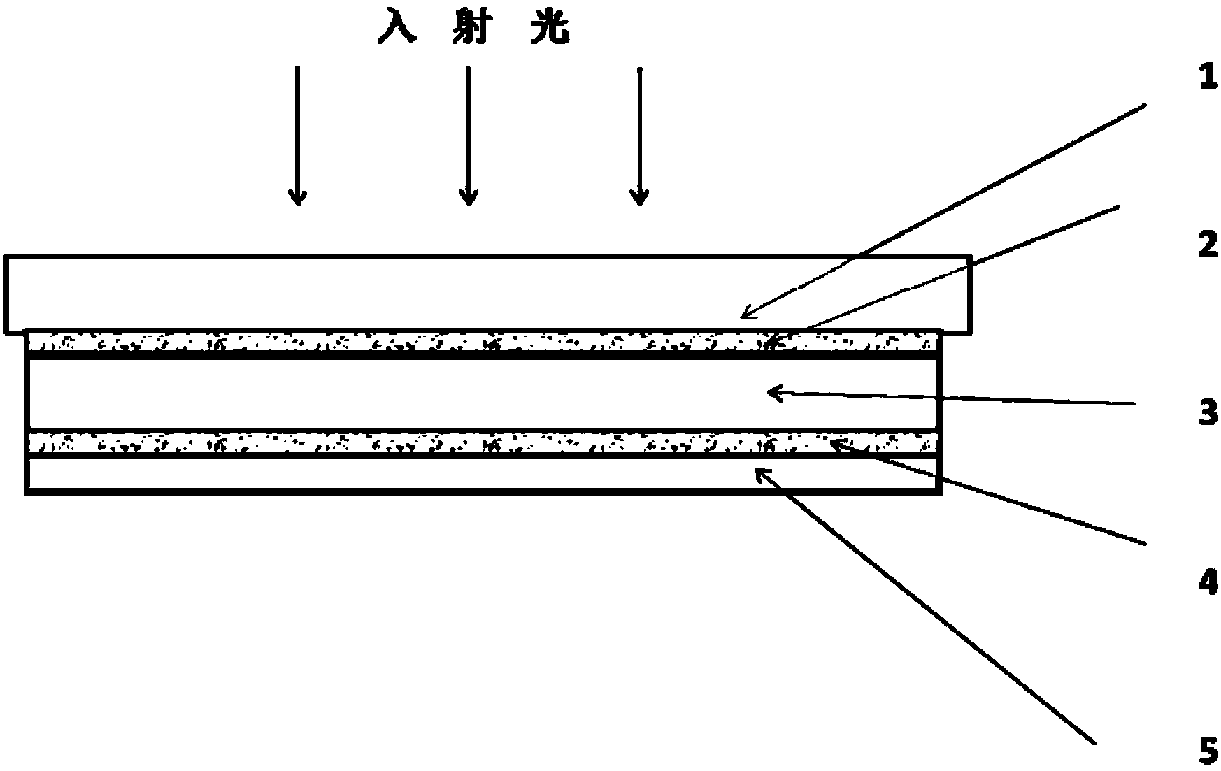
[0074] The all-solid-state perovskite microcrystalline silicon composite thin film solar cell is composed of a transparent conductive substrate 1, an oxide semiconductor thin film layer 2, a perovskite light absorbing layer 3, a microcrystalline silicon hole transport layer 4 and a back electrode 5. This implementation The transparent conductive substrate 1 of the example is SnO doped with fluorine 2 A transparent conductive glass substrate, the oxide semiconductor thin film layer 2 is a titanium dioxide thin film layer, and the back electrode 5 is an aluminum back electrode, the titanium dioxide thin film layer is coated on a transparent conductive substrate, prepared on a transparent conductive substrate coated with a titanium dioxide thin film The perovskite light absorbing layer and the microcrystalline silicon hole transport layer are deposited on the perovskite light absorbing layer to form an all-solid perovskite microcrystalline silicon composite film, and the aluminum ...

Embodiment 2

[0102] The all-solid-state perovskite microcrystalline silicon composite thin film solar cell is composed of a transparent conductive substrate 1, an oxide semiconductor thin film layer 2, a perovskite light absorbing layer 3, a microcrystalline silicon hole transport layer 4 and a back electrode 5. This implementation The transparent conductive substrate 1 of the example is SnO doped with fluorine 2 A transparent conductive glass substrate, the oxide semiconductor thin film layer 2 is a titanium dioxide thin film layer, and the back electrode 5 is an aluminum back electrode, the titanium dioxide thin film layer is coated on a transparent conductive substrate, prepared on a transparent conductive substrate coated with a titanium dioxide thin film The perovskite light absorbing layer and the microcrystalline silicon hole transport layer are deposited on the perovskite light absorbing layer to form an all-solid perovskite microcrystalline silicon composite film, and the aluminum ...

Embodiment 3

[0117] The all-solid-state perovskite microcrystalline silicon composite thin film solar cell is composed of a transparent conductive substrate 1, an oxide semiconductor thin film layer 2, a perovskite light absorbing layer 3, a microcrystalline silicon hole transport layer 4 and a back electrode 5. This implementation The transparent conductive substrate 1 of the example is SnO doped with fluorine 2 A transparent conductive glass substrate, the oxide semiconductor thin film layer 2 is a titanium dioxide thin film layer, and the back electrode 5 is an aluminum back electrode, the titanium dioxide thin film layer is coated on a transparent conductive substrate, prepared on a transparent conductive substrate coated with a titanium dioxide thin film The perovskite light absorbing layer and the microcrystalline silicon hole transport layer are deposited on the perovskite light absorbing layer to form an all-solid perovskite microcrystalline silicon composite film, and the aluminum ...


PUM

PropertyMeasurementUnit
Thicknessaaaaaaaaaa
Thicknessaaaaaaaaaa
Thicknessaaaaaaaaaa

Abstract

The invention discloses an all solid state perovskite microcrystalline silicon composite solar battery and a preparation method thereof, and relates to a semiconductor device specially suitable for converting light energy into electric energy. The all solid state perovskite microcrystalline silicon composite solar battery is composed of a transparent conducting substrate, an oxide semiconductor film layer, a perovskite light absorption layer, a microcrystalline silicon hole transport layer and a back electrode. The preparation method of the all solid state perovskite microcrystalline silicon composite solar battery includes: preparing the perovskite light absorption layer on the transparent conducting substrate coated with an oxide semiconductor film; depositing the microcrystalline silicon hole transport layer on the perovskite light absorption layer so as to form an all solid state perovskite microcrystalline silicon composite film; compositing perovskite light absorption layer material and P type microcrystalline silicon material in matching mode. The all solid state perovskite microcrystalline silicon composite solar battery prepared from the above preparation method simultaneously overcomes the defects that an existing perovskite solar battery is poor in stability and expensive in cost due to the fact that organic hole transport material is used on the existing perovskite solar battery, and the defects that preparation costs are high and photoelectric conversion efficiency is low, caused by low preparation speed of a microcrystalline silicon thin film solar battery.

Description

technical field [0001] The technical solution of the invention relates to a semiconductor device specially suitable for converting light energy into electric energy, specifically an all-solid-state perovskite microcrystalline silicon composite solar cell and a preparation method thereof. Background technique [0002] In the case of decreasing fossil fuels, solar energy, as an emerging renewable energy source, has become an important part of energy used by human beings and has been continuously developed. Solar power generation is a major form of solar energy utilization. Low-cost, high-efficiency and long-term stable solar cells are the basis for large-scale photoelectric conversion using solar energy. [0003] A type of solar cell that is currently developing rapidly is the perovskite solar cell, which is composed of a conductive substrate, an electron transport material, a perovskite light absorbing layer, an organic hole transport material, and a metal electrode. The per...

Claims


Application Information

Patent Timeline
IPC IPC(8): H01L51/42H01L51/44H01L51/48
CPCH10K30/00H10K30/80Y02E10/549
Inventor 田汉民吴亚美杨瑞霞金慧娇王伟杨帆张明兰赵红东
Owner HEBEI UNIV OF TECH
Why Eureka
Try Eureka