A low-voltage diffusion process for high square resistance crystalline silicon cells
A crystalline silicon cell and diffusion process technology, applied in the field of diffusion process, can solve problems such as the proportion of defective wafers, affecting the cost of cell preparation, and reducing the uniformity of longitudinal doping concentration of diffused PN junctions.
- Summary
- Abstract
- Description
- Claims
- Application Information
AI Technical Summary
Problems solved by technology
Method used
Image
Examples
Embodiment 1
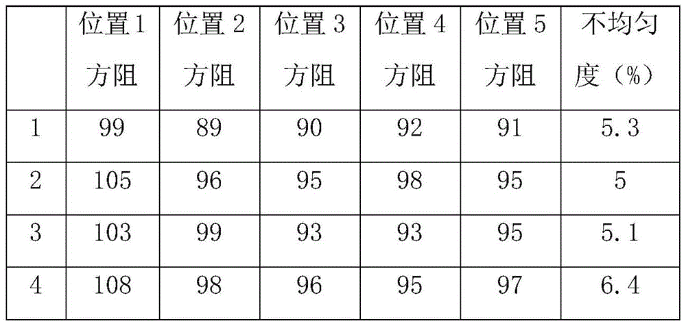
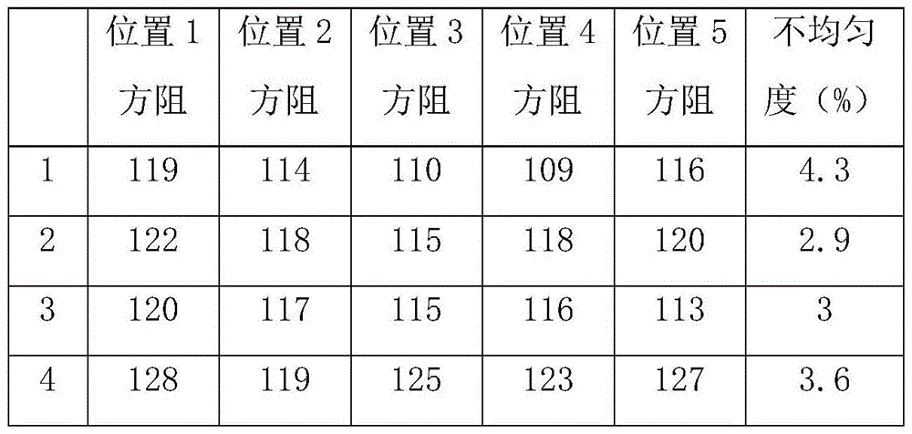
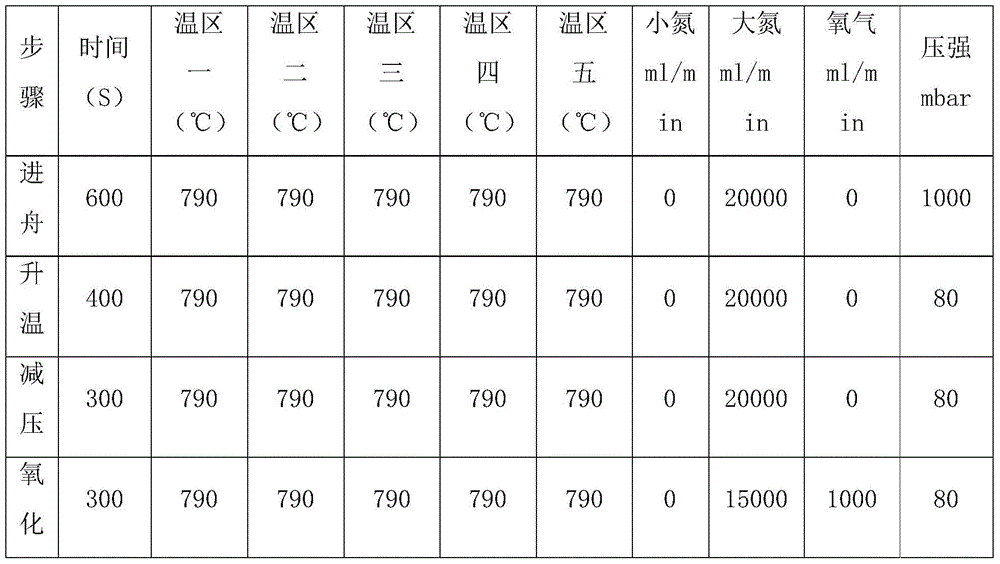
[0039] In this embodiment, the diffusion furnace is selected from the 48th Research Institute of China Electronics Technology Group Corporation. There are five heaters in the diffusion furnace, which are divided into five temperature zones. This diffusion process is carried out under the premise of keeping other process steps unchanged, and the first three steps of diffusion are as follows (Table 3):
[0040] table 3:
[0041]
[0042] A two-step temperature rise diffusion method is adopted, and the specific diffusion steps are as follows:
[0043] In the first step, the diffusion temperature is maintained at a low level, and the reaction rate is very slow, so as to realize pre-diffusion and deposit phosphorus source on the surface.
[0044] The second step is to increase the temperature and diffuse to promote the decomposition of the phosphorus source and the diffusion into the silicon, and at the same time increase the concentration of the phosphorus source on the surfac...
PUM
 Abstract
Description
Claims
Application Information


