
Preparation method of GaN-based LED epitaxial wafer enhancing luminescence efficiency

A technology for LED epitaxial wafers and luminous efficiency, applied in electrical components, circuits, semiconductor devices, etc., can solve problems such as increasing process complexity, and achieve the effect of improving external quantum efficiency, simple method and reducing Stark effect.

Active Publication Date: 2015-03-04
XIAMEN CHANGELIGHT CO LTD
View PDF4 Cites 2 Cited by
  • Summary
  • Abstract
  • Description
  • Claims
  • Application Information

AI Technical Summary

Problems solved by technology

The preparation of semi-polar or non-polar GaN templates and lateral epitaxial growth technology increase the complexity of the process
[0007] In summary, in the prior art, there are still many technical difficulties in the preparation of GaN-based LED epitaxial wafers with low cost and high luminous efficiency.

Method used


Image

  • Preparation method of GaN-based LED epitaxial wafer enhancing luminescence efficiency
  • Preparation method of GaN-based LED epitaxial wafer enhancing luminescence efficiency
  • Preparation method of GaN-based LED epitaxial wafer enhancing luminescence efficiency

Examples


Embodiment 1

[0037] Using MOCVD equipment to grow GaN-based LEDs, using a 2-inch C-face no-clean sapphire substrate, the epitaxy steps mainly include:

[0038] 1. Raise the temperature of the reaction chamber to 1200°C, the pressure of the reaction chamber is 100mbar, in H 2 Bake the sapphire substrate under atmosphere for 300s.

[0039] 2. Reduce the temperature of the reaction chamber to 560°C and feed NH 3 , nitrided substrate 120s.

[0040] 3. Adjust the reaction chamber pressure to 600 mbar, and feed Ga source and NH 3 , The ratio of V / III is 1200, and a 25nm GaN buffer layer is grown at 560°C.

[0041] 4. Increase the temperature of the reaction chamber to 1100°C, adjust the pressure of the reaction chamber to 250mbar, and feed Ga source and NH 3 , The ratio of Ⅴ / Ⅲ is 1500, and a 2000nm non-intentionally doped GaN layer is grown.

[0042] 5. Ga source, NH 3 and silane, the ratio of V / III is 1500, and a 2500nm N-type doped GaN layer is grown, and the N-type doping concentration is...

Embodiment 2

[0052] The difference between this embodiment and the first embodiment is that in this embodiment, during the interrupted growth process, the NH 3 traffic methods such as Figure 5 Shown, specifically: keep NH within 0-15s 3 Normal flow into the reaction chamber, within 15-65s, close the NH 3 , within 65-80s, turn on NH again 3 , keep NH 3 Normal flow into the reaction chamber.

Embodiment 3

[0054] The difference between this embodiment and the first embodiment is that in this embodiment, during the interrupted growth process, the NH 3 The flow adopts pulse type, such as Figure 6 shown, specifically: pulse on NH 3 and off NH 3 The times are 5s and 15s respectively, repeating 4 cycles in total.


PUM

PropertyMeasurementUnit
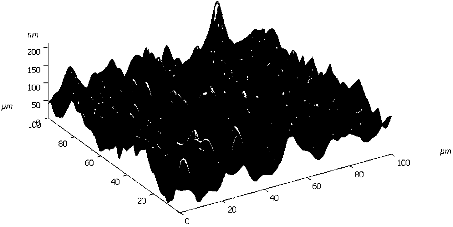
Surface roughnessaaaaaaaaaa
Average heightaaaaaaaaaa

Abstract

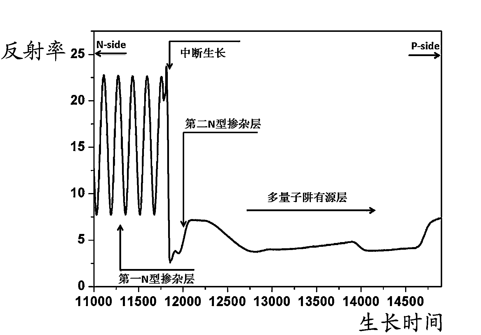
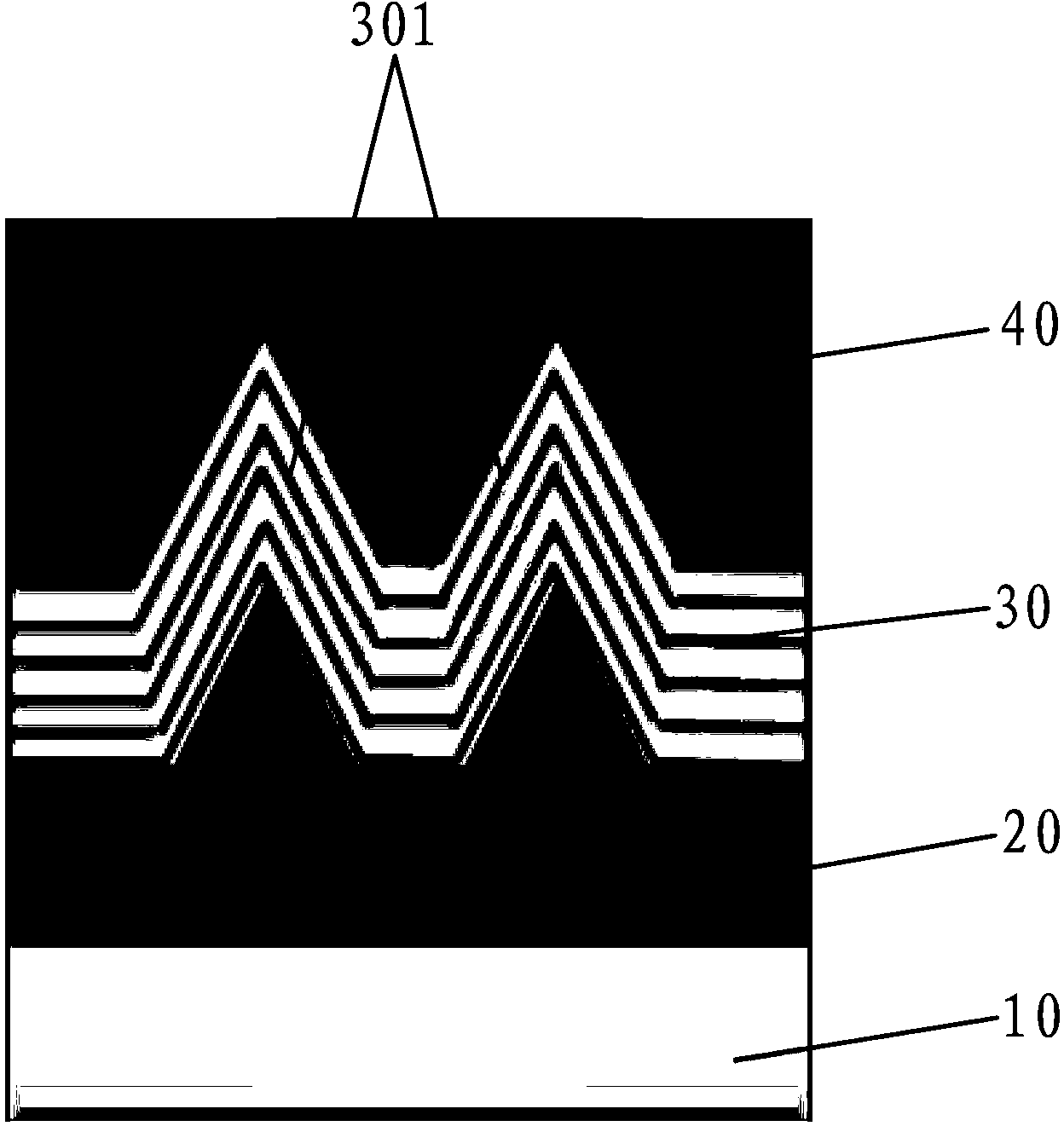
The invention discloses a preparation method of a GaN-based LED epitaxial wafer enhancing luminescence efficiency. The preparation method comprises the following steps that a buffer layer, an unintentional doping layer, a first N-type doping layer, a second N-type doping layer, a InGaN / GaN multi-quantum well active layer, an electron blocking layer, a P-type doping layer and a contact layer are grown on a substrate in turn; after the first N-type doping layer is grown completely, an organic source is closed, piping of NH3 into a reaction chamber is reduced or stopped and growing is stopped for 10-200s under the atmosphere of H2 or N2 so that the first N-type doping layer with a rough surface is acquired. LED internal quantum efficiency and external quantum efficiency can be enhanced simultaneously. Besides, the preparation method is simple and preparation cost is relatively low.

Description

technical field [0001] The invention relates to the technical field of GaN-based LED epitaxial wafer preparation, in particular to a GaN-based LED epitaxial wafer preparation method for improving luminous efficiency. Background technique [0002] GaN-based LED has the advantages of small size, long life, low power consumption, high brightness and easy integration, etc., and has entered the field of general lighting. high. Therefore, improving the brightness of GaN-based LEDs has become a key issue that needs to be solved urgently. [0003] In the existing technology, improving the brightness of GaN-based LEDs mainly lies in the improvement of internal quantum efficiency and external quantum efficiency, including optimization of epitaxial structure, improvement of crystal quality, processing and roughening of graphics substrate, optimization of chip structure, etc. . [0004] Due to the large difference between the refractive index of GaN material and air, the light emitte...

Claims


Application Information

Patent Timeline
IPC IPC(8): H01L33/32H01L33/06
CPCH01L33/007H01L33/06H01L33/22H01L33/32
Inventor 卓祥景林志伟陈凯轩蔡建九张永姜伟林志园尧刚
Owner XIAMEN CHANGELIGHT CO LTD
Learn More