Polycrystalline silicon crystal orientation degree evaluation method, polycrystalline silicon rod selection method, polycrystalline silicon rod, polycrystalline silicon ingot, and polycrystalline silicon fabrication method

A technology of crystal orientation and polysilicon rods, which is applied in the directions of crystal growth, single crystal growth, single crystal growth, etc., can solve the problem that microcrystals cannot be melted, and achieve the effect of suppressing melting residue and stabilizing manufacturing

Active Publication Date: 2015-03-04
SHIN ETSU CHEM CO LTD
View PDF11 Cites 6 Cited by
  • Summary
  • Abstract
  • Description
  • Claims
  • Application Information

AI Technical Summary

Problems solved by technology

[0004] In addition, in Patent Document 2, in the process of manufacturing polycrystalline silicon rods (polycrystalline silicon rods) by the Siemens method, needle-shaped crystals sometimes precipitate in the rods, and when the polycrystalline silicon rods are used to grow single crystal silicon by the FZ method, It has been pointed out that there is a problem that each crystallite cannot be melted uniformly corresponding to its size due to the above-mentioned non-uniform microstructure, and the unmelted crystallites pass through the molten region as solid particles to the single-crystal rod rod and thus appear as unmelted crystals. Particles are introduced to the solidification surface of the single crystal, thereby causing defect formation

Method used


Image

  • Polycrystalline silicon crystal orientation degree evaluation method, polycrystalline silicon rod selection method, polycrystalline silicon rod, polycrystalline silicon ingot, and polycrystalline silicon fabrication method
  • Polycrystalline silicon crystal orientation degree evaluation method, polycrystalline silicon rod selection method, polycrystalline silicon rod, polycrystalline silicon ingot, and polycrystalline silicon fabrication method
  • Polycrystalline silicon crystal orientation degree evaluation method, polycrystalline silicon rod selection method, polycrystalline silicon rod, polycrystalline silicon ingot, and polycrystalline silicon fabrication method

Examples


Embodiment

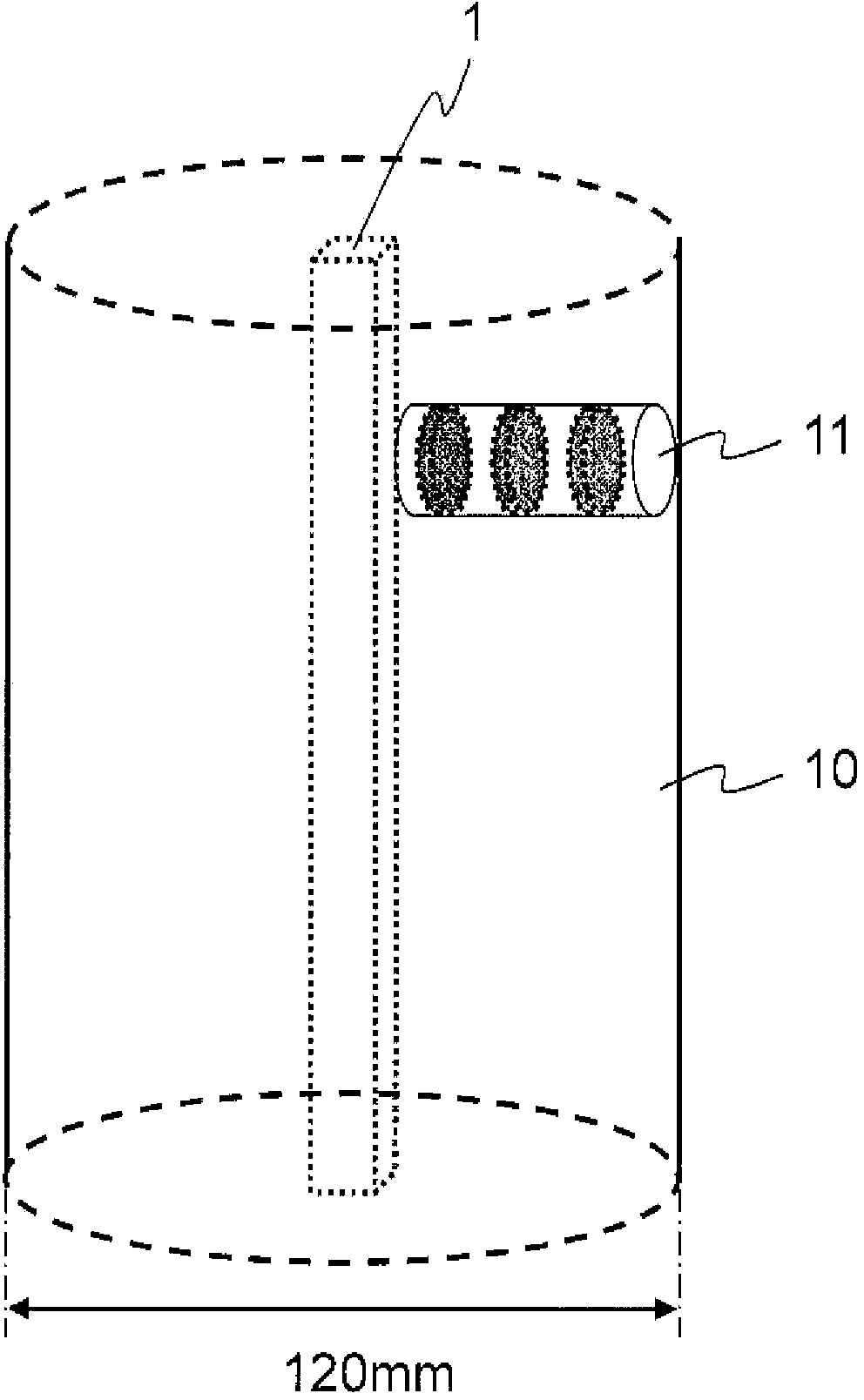
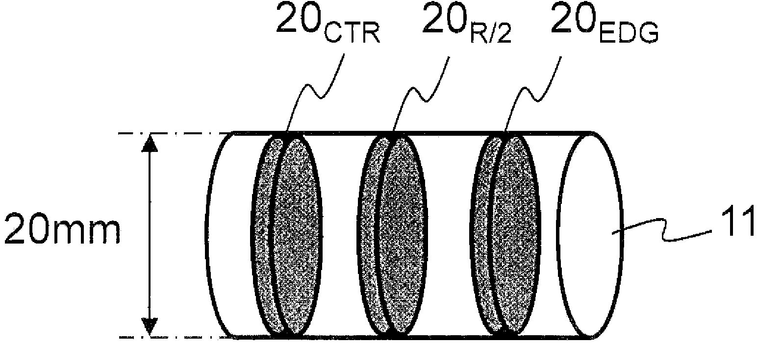
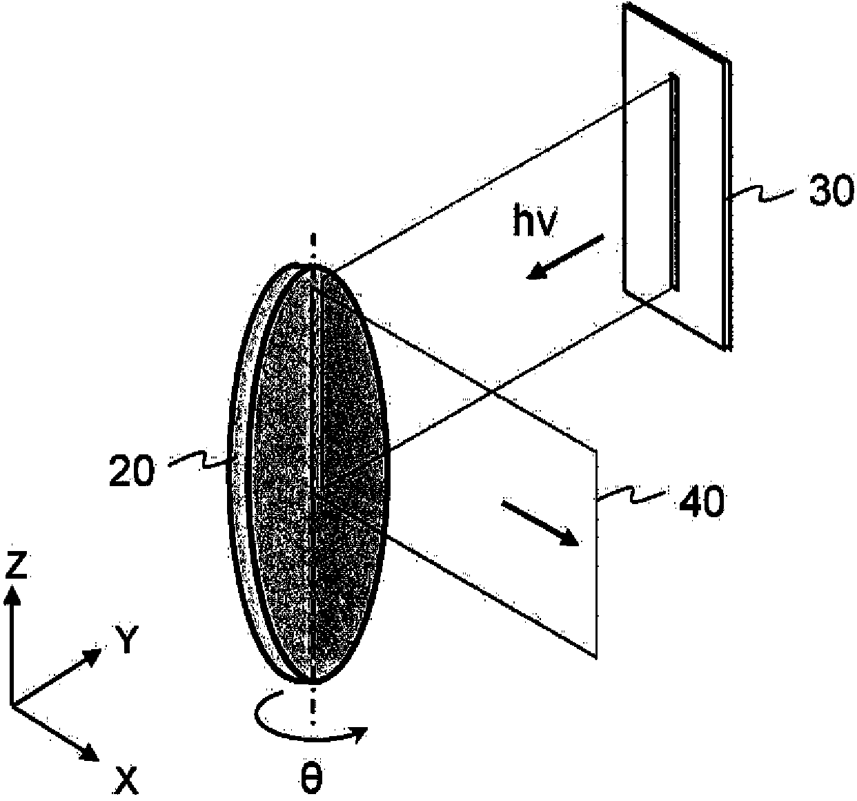
[0071] Prepare six polysilicon rods grown under different precipitation conditions. For these polycrystalline silicon rods (silicon rods A ~ F), respectively, from Figure 1A and 1B Select a circular plate-shaped sample with a thickness of about 2 mm (20 CTR 、20 EDG 、20 R / 2 ),pass Figure 6 With the measurement system shown, the φ scan charts of the Miller index surfaces and are obtained. In addition, the diameter of the disk-shaped sample 20 was about 20 mm.

[0072] Table 1 summarizes the diffraction intensity of the baseline (BL) obtained from these polycrystalline silicon rods for each disk-shaped sample, and whether or not crystal lines disappeared when the polycrystalline silicon rods were grown by the FZ method for single crystal silicon rods.

[0073] [Table 1]

[0074]

[0075] For silicon rod A, the value obtained by dividing the maximum value of the multiple baseline diffraction intensity values ​​for the Miller index surface by the mini...


PUM

PropertyMeasurementUnit
diameteraaaaaaaaaa

Abstract

The present invention provides a technology which selects, with high levels of quantitativity and reproducibility, a desirable polycrystalline silicon as a raw material for single crystal silicon fabrication, and contributes to stable fabrication of the single crystal silicon. When evaluating a degree of orientation of a crystal of a polycrystalline silicon by x-ray diffraction: an adopted disc-shaped sample (20) is positioned in a location in which Bragg reflection from a mirror index face <hkl> is detected; an in-plane rotation is carried out at a rotation angle (Phi) with the center of the disc-shaped sample (20) as the center of rotation thereof, such that an x-ray projection region which is defined by a slit Phi scans a primary surface of the disc-shaped sample (20); a chart is derived which denotes a rotation angle (Phi) dependency of the disc-shaped sample (20) of the Bragg reflection intensity from the Miller index face <hkl>; a baseline is derived from the chart; and a value of an intensity of diffraction of the baseline is employed as an evaluation index of the degree of orientation of the crystal.

Description

technical field [0001] The present invention relates to a method for evaluating the degree of crystal orientation of polycrystalline silicon and a method for selecting a non-oriented polycrystalline silicon rod or polycrystalline silicon block suitable as a raw material for stably producing single crystal silicon using the method. Background technique [0002] Monocrystalline silicon, which is indispensable in the manufacture of semiconductor devices, is grown by the CZ method or the FZ method, and polycrystalline silicon rods and polycrystalline silicon blocks are used as raw materials for this process. Such polysilicon materials are often produced by the Siemens method (see Patent Document 1 and the like). The Siemens method refers to a method in which a silane raw material gas such as trichlorosilane or monosilane is brought into contact with a heated silicon core wire, thereby depositing polysilicon on the silicon core by CVD (Chemical Vapor Deposition) method. A method...

Claims


Application Information

Patent Timeline
Patent Type & Authority Applications(China)
IPC IPC(8): G01N23/20C01B33/02C01B33/035
CPCC01B33/021G01N2223/606C30B13/00C30B29/06G01N23/207G01N2223/3306C01B33/035C01B33/02G01N23/20C30B29/605
Inventor 宫尾秀一冈田淳一祢津茂义
Owner SHIN ETSU CHEM CO LTD
Why Eureka
Try Eureka