Preparation method of sub-wavelength silicon nanowire array
A silicon nanowire array and sub-wavelength technology, which is applied in the field of nanomaterials, achieves the effects of reducing production costs, great application prospects, and good anti-reflection characteristics
- Summary
- Abstract
- Description
- Claims
- Application Information
AI Technical Summary
Problems solved by technology
Method used
Image
Examples
Embodiment 1
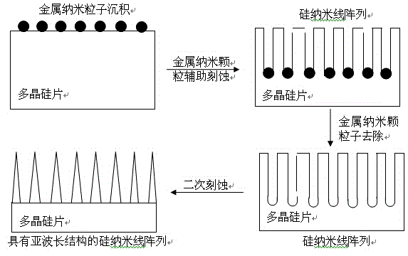
[0027] The preparation method of the sub-wavelength silicon nanowire array described in this embodiment specifically comprises the following steps:
[0028] (1) Set the size to 156×156mm 2 1. A commercial solar-grade polysilicon wafer with a doping type of p-type, a resistance of 1Ω, and a thickness of 220 μm was ultrasonically cleaned with acetone, toluene, ethanol, and deionized water for 10 minutes;
[0029] (2) put in H 2 SO 4 and H 2 o 2Soak for 1 minute in a solution with a volume ratio of 3:1, then soak for 10 minutes in a hydrofluoric acid solution with a concentration of 10 wt%, take it out and rinse it with a large amount of deionized water for later use;
[0030] (3) Prepare 500ml HF / AgNO 3 Etching solution, HF and AgNO 3 The concentrations are 2.3mol / L and 5mol / L respectively; put the cleaned polysilicon wafer into the etching solution, move it to a dark room and let it stand for 50 minutes to obtain a silicon nanowire array with metal ions;
[0031] (4) Tak...
Embodiment 2
[0034] The preparation method of the sub-wavelength silicon nanowire array described in this embodiment specifically comprises the following steps:
[0035] (1) Set the size to 156×156mm 2 1. A commercial solar-grade polysilicon wafer with a doping type of p-type, a resistance of 2Ω, and a thickness of 210 μm was ultrasonically cleaned with acetone, toluene, ethanol, and deionized water for 10 minutes;
[0036] (2) put in H 2 SO 4 and H 2 o 2 Soak it in a solution with a volume ratio of 3:1 for 10 minutes, then soak it in a hydrofluoric acid solution with a concentration of 0.1wt% for 120 minutes, take it out and wash it with a large amount of deionized water for later use;
[0037] (3) Prepare 500ml HF / H 2 PtCl 6 Etching solution, HF and H 2 PtCl 6 The concentrations are 15mol / L and 5mol / L respectively; put the cleaned polysilicon wafer into the etching solution and let it stand for 5min to obtain a silicon nanowire array with metal ions;
[0038] (4) Take out the si...
Embodiment 3
[0041] The preparation method of the sub-wavelength silicon nanowire array described in this embodiment specifically comprises the following steps:
[0042] (1) Set the size to 156×156mm 2 1. A commercial solar-grade polysilicon wafer with a doping type of p-type, a resistance of 3Ω, and a thickness of 180 μm was ultrasonically cleaned with acetone, toluene, ethanol, and deionized water for 10 minutes;
[0043] (2) put in H 2 SO 4 and H 2 o 2 Soak in a solution with a volume ratio of 3:1 for 2 minutes, then soak in a hydrofluoric acid solution with a concentration of 5wt% for 20 minutes, take it out and wash it with a large amount of deionized water for subsequent use;
[0044] (3) Prepare 500ml HF / KAuCl 4 Etching solution, HF and KAuCl 4 The concentrations are 0.1mol / L and 10mol / L respectively; put the cleaned polysilicon wafer into the etching solution, then move it to the dark room and let it stand for 600min;
[0045] (4) After that, take out the silicon nanowire ar...
PUM
| Property | Measurement | Unit |
|---|---|---|
| Thickness | aaaaa | aaaaa |
| Thickness | aaaaa | aaaaa |
| Thickness | aaaaa | aaaaa |
Abstract
Description
Claims
Application Information
 - R&D Engineer
- R&D Manager
- IP Professional
- Industry Leading Data Capabilities
- Powerful AI technology
- Patent DNA Extraction
Browse by: Latest US Patents, China's latest patents, Technical Efficacy Thesaurus, Application Domain, Technology Topic, Popular Technical Reports.
© 2024 PatSnap. All rights reserved.Legal|Privacy policy|Modern Slavery Act Transparency Statement|Sitemap|About US| Contact US: help@patsnap.com


