Transistor and transistor forming method

A technology of transistors and semiconductors, which is applied in the manufacture of transistors, semiconductor devices, semiconductor/solid-state devices, etc., can solve the problems of transistors prone to latch-up effect, low transistor operation speed, short channel effect, etc., to avoid latch-up effect, Effect of avoiding warpage effect and improving reliability

Active Publication Date: 2015-03-18
SEMICON MFG INT (SHANGHAI) CORP
View PDF3 Cites 0 Cited by
  • Summary
  • Abstract
  • Description
  • Claims
  • Application Information

AI Technical Summary

Problems solved by technology

[0004] However, the above method may lead to short channel effect (SCE: Short Channel Effect). In order to alleviate the short channel effect, in the prior art, after the lightly doped source and drain regions are formed, the Pocket implantation is performed on both sides of the channel region, and the type of impurity ions implanted in the pocket region is opposite to the type of impurity ions implanted in the lightly doped source and drain regions, so that the lightly doped source and drain regions are close to the channel The depletion region on both sides of the channel region is narrowed, which can alleviate the short channel effect
[0005] Although the introduction of technologies such as LDD and Pocket can improve the performance of the transistor to a certain extent, the electrical performance of the transistor formed by the existing technology still needs to be improved, such as the operation speed of the transistor is low, the power consumption is high, and the latch-up is prone to occur in the transistor effect

Method used


Image

  • Transistor and transistor forming method
  • Transistor and transistor forming method
  • Transistor and transistor forming method

Examples


Embodiment Construction

[0038] It can be seen from the background art that the transistors formed in the prior art have problems such as low operating speed, high power consumption, and latch-up effect.

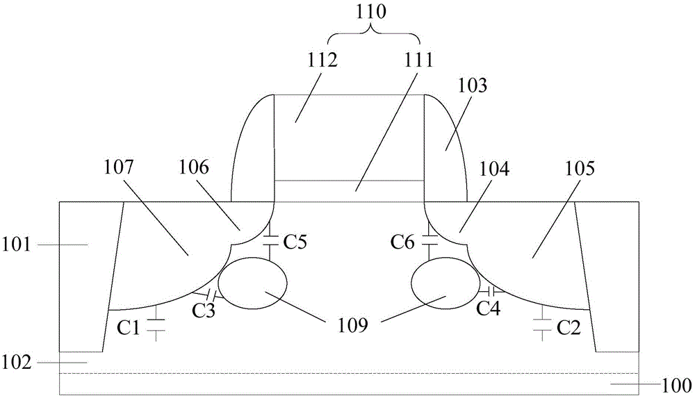
[0039] For this reason, the formation process of transistors is studied, and it is found that the formation process of transistors includes the following steps, please refer to figure 1 , figure 1 Schematic diagram for forming a cross-section of a transistor:

[0040] providing a semiconductor substrate 100, forming a well region 102 in the semiconductor substrate 100, and forming a shallow trench isolation structure 101 in the semiconductor substrate 100 after the well region 102 is formed;

[0041] Forming a gate structure 110 on the surface of the semiconductor substrate 100, the gate structure 110 includes a gate dielectric layer 111 on the surface of the semiconductor substrate 100 and a gate conductive layer 112 on the surface of the gate dielectric layer 111;

[0042] Lightly doped regions ( ...


PUM


Abstract

The invention relates to a transistor and a transistor forming method, wherein the transistor forming method comprises the following steps that a semiconductor substrate is provided; at least two grooves are formed in the semiconductor substrate; insulation layers filling the grooves are formed in the grooves, and in addition, the tops of the insulation layers are set to be lower than the surface of the semiconductor substrate; epitaxial layers are formed on the surface and the side wall of the semiconductor substrate higher than the tops of the isolation layers, and in addition, the epitaxial layers are enabled to cover the partial isolation layers arranged at the two sides of the semiconductor substrate; a well region is formed in the semiconductor substrate and the epitaxial layers; a gate electrode structure is formed on the surface of each epitaxial layer, wherein each gate electrode structure comprises a gate dielectric layer covering the surface of the corresponding epitaxial layer and a gate conducting layer positioned on the top of the grate dielectric layer; light doping regions are formed in the epitaxial layers arranged at the two sides of the grate conducting layers; a heavy doping region is formed in each light doping region, and in addition, the heavy doping regions and the well region are isolated by the light doping regions and the isolation layers. The transistor formed by the method provided by the invention has low power consumption, the operation speed is high, the groove dimension is small, and in addition, the warping effect can be effectively eliminated.

Description

technical field [0001] The invention relates to the field of semiconductor manufacturing, in particular to a transistor and a method for forming the transistor. Background technique [0002] With the continuous improvement of the integration of semiconductor devices, the feature size is gradually reduced, the length of the channel of the transistor is also gradually reduced, and the thickness of the gate dielectric layer is also continuously reduced. Since the gate voltage will not continue to decrease (currently at least 1V ), so that the electric field intensity received by the gate oxide layer becomes larger, and time-dependent dielectric breakdown (TDDB: Time Dependent Dielectric Breakdown) is also more likely to occur, and it is easy to form a hot carrier injection effect (HCI: Hot Carrier Injection ). [0003] In the prior art, the lightly doped source and drain (LDD: Lightly Doped Drain) ion implantation is usually used to optimize the hot carrier injection effect. B...

Claims


Application Information

Patent Timeline
Patent Type & Authority Applications(China)
IPC IPC(8): H01L29/78H01L27/088H01L21/336H01L21/8234
CPCH01L29/0603H01L29/0688H01L29/66492H01L29/66553H01L29/7834
Inventor 王海强蒲贤勇汪铭
Owner SEMICON MFG INT (SHANGHAI) CORP
Why Eureka
Try Eureka