Method of making electrical test structure for detecting vias

A technology for detecting through-holes and test structures, which is applied in semiconductor/solid-state device testing/measurement, circuits, electrical components, etc., and can solve the problem of increasing process complexity and process cost, increasing requirements, and small photolithography process window, etc. problems, to achieve the effect of improving lithography resolution and lithography precision, improving lithography resolution, and expanding the process window

CN104465446BActive Publication Date: 2018-05-01SHANGHAI INTEGRATED CIRCUIT RES & DEV CENT
3 Cites 0 Cited by

Patent Information

Authority / Receiving Office
CN · China
Patent Type
Patents(China)
Current Assignee / Owner
Publication Date
2018-05-01

Smart Images

  • Figure 1
    Figure 1
  • Figure 2
    Figure 2
  • Figure 3
    Figure 3
Patent Text Reader

Abstract

The invention provides a manufacturing method of an electric testing structure for detecting through holes. When a layout is designed, a through hole graph is connected with the overlapping area of a plurality of adjacent metal graphs in an intersection mode, the through hole graph size is larger than the target through hole size, a through hole pattern subsequently formed in optical resist is enabled to be larger than a target through hole graph in size, and therefore a photo-etched technical window is widened, and the photoetching resolution and the photoetching precision are improved; besides, a hard mask layer serves as a mask, and an upper layer metal pattern in the hard mask layer is etched into an etched barrier layer and an upper dielectric layer so that a target through hole pattern can be formed; the target through hole size is determined by the size of the upper metal pattern in the hard mask layer and the through hole size jointly and not determined by the size of the through hole graph in the optical resist, and therefore target through holes with smaller intervals can be obtained without splitting the through hole graph, the technical window is widened, and the photoetching resolution ratio is increased.
Need to check novelty before this filing date? Find Prior Art

Description

technical field

[0001] The invention relates to the technical field of semiconductors, in particular to a preparation method of an electrical test structure for detecting through-hole resistance and electric leakage. Background technique

[0002] According to Moore's law, the critical dimensions of semiconductor devices continue to shrink, and the line width of interconnect lines also continues to decrease. In order to obtain lower resistance and capacitance in the dielectric film of interconnect lines, the process generation of 0.13um and below is gradually changed from Copper interconnects have replaced aluminum interconnects. Due to the difficulty of dry etching metal copper, a dual damascene process is generally used to form copper interconnects and vias.

[0003] In the copper interconnection process, resistance and leakage are the most concerned parts of the process. The size of the resistance affects the speed of the device, and the size of the leakage affects the re...

Examples

preparation example Construction

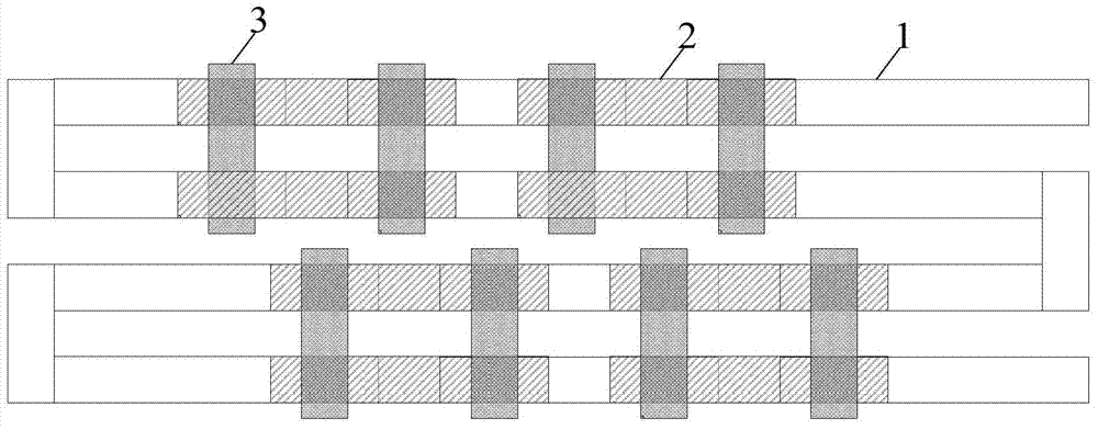
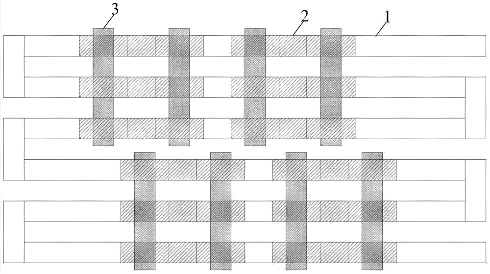
[0037] The layout adopted in the preparation process of the test structure of the present invention includes: a plurality of metal patterns arranged at a certain distance and a through-hole pattern cross-connected with a plurality of adjacent metal patterns; wherein, each metal pattern consists of an upper metal pattern and the lower metal pattern; the end of the upper metal pattern overlaps with the end of the adjacent lower metal pattern to form an overlapping area; the through hole pattern is connected to the overlapping area on a plurality of adjacent metal patterns, and through The size of the hole pattern is larger than the size of the top of the target via.

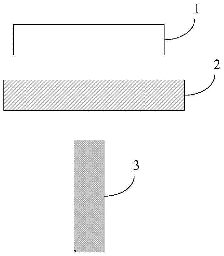
[0038] For each structure in the layout of the test structure in an embodiment of the present invention, please refer to figure 1 , the upper metal pattern, the lower metal pattern and the through-hole pattern are all strips; the size of the through-hole pattern is larger than the size of the target through-hole, s...