Semiconductor contact hole etching method

A contact hole and semiconductor technology, applied in semiconductor/solid-state device manufacturing, electrical components, circuits, etc., can solve the problems of excessive lithography overlay deviation, affecting breakdown voltage and contact resistance, device failure, etc., to achieve etching Accurate, improve electrical performance, reduce loss effect

Inactive Publication Date: 2015-03-25
SHANGHAI HUALI MICROELECTRONICS CORP
View PDF3 Cites 4 Cited by
  • Summary
  • Abstract
  • Description
  • Claims
  • Application Information

AI Technical Summary

Problems solved by technology

Whether it is SiN or SiON-SiN composite etch barrier layer, under the pressure of Moore's law on the chip area, its thickness becomes smaller with the channel length, so that the interlayer dielectric layer (ILD) to the contact hole The selection ratio of the etch stop layer (CESL) puts forward higher requirements, but whether the photolithography scheme such as PR (photoresist) or HM (hard mask) is used, the interlayer dielectric layer (ILD) is the most important for contact hole etching. There is a limit to the improvement of the selectivity ratio of the layer (CESL), so when there is a process miss in the current layer, such as excessive lithography deviation or insufficient metal silicide thickness, it will affect the shallow trench isolation structure (STI) and the bottom The silicide layer causes greater loss, which affects the corresponding parameters such as breakdown voltage and contact resistance, causing device failure

Method used


Image

  • Semiconductor contact hole etching method
  • Semiconductor contact hole etching method

Examples


Embodiment Construction

[0030] The present invention will be further described below in conjunction with the accompanying drawings and specific embodiments, but not as a limitation of the present invention.

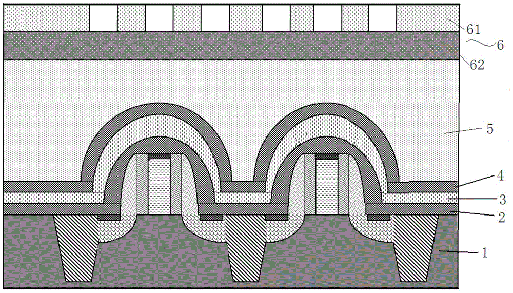
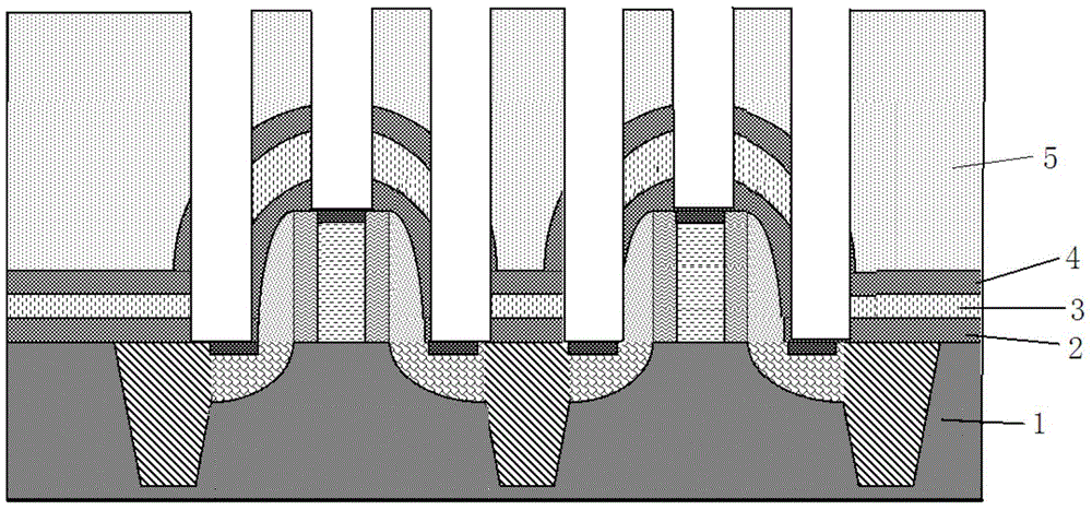
[0031] Such as figure 1 , 2 As shown, a semiconductor contact hole etching method is characterized in that: comprising the following steps

[0032] Step 1, providing a substrate 1 on which a plurality of conductive structures are formed. In the semiconductor field, the base 1 is a semiconductor substrate, on which gates and sidewalls are formed; AA (active area, active area) regions are defined in the substrate, and shallow trenches pass between adjacent AA regions. Isolation area (STI) for isolation,. A source and a drain are respectively formed in the substrate on both sides of the bottom of the gate, and metal silicon oxide is formed on the top of the gate and the top of the source / drain.

[0033] Step 2, forming a first SiN layer covering the substrate and the conductive structure on the...


PUM


Abstract

The invention relates to a semiconductor contact hole etching method achieved through a sandwich structure. The method includes the steps of providing a substrate, wherein a plurality of electric conduction structures are formed on the substrate; forming a first SiN layer covering the substrate and the electric conduction structures on the substrate; forming an SiO2 layer on the first SiN layer; forming a second SiN layer on the SiO2 layer; forming an ILD layer of the SiO2 layer on the second SiN layer through deposition; flattening the ILD layer and forming an ILD cap layer on the surface of the ILD layer, wherein the ILD cap layer sequentially comprises a photoetching adhesive layer and an anti-reflection coating from top to bottom; forming a contact hole pattern in the photoetching adhesive layer; conducting etching through the contact hole pattern so that all the electric conduction structures and source/drain electrodes located on the two sides of the electric conduction structures can be exposed. The method has the advantages that the adoption of the single-medium SiN or double-layer media is avoided, and the number of silicon oxides on the surface of the substrate and the number of consumed STI layers are decreased.

Description

technical field [0001] The present invention relates to the field of semiconductor manufacturing. Specifically, it relates to an etching method using a semiconductor material with a sandwich structure as an etching stop layer for a contact hole. Background technique [0002] The choice of etch stop layer for contact hole etching is mostly a single dielectric SiN layer. There are also cases in the industry where SiON or SiN-SiON composite layers are used instead of SiN due to high requirements for leakage. Whether it is SiN or SiON-SiN composite etch barrier layer, under the pressure of Moore's law on the chip area, its thickness becomes smaller with the channel length, so that the interlayer dielectric layer (ILD) to the contact hole The selection ratio of the etch stop layer (CESL) puts forward higher requirements, but whether the photolithography scheme such as PR (photoresist) or HM (hard mask) is used, the interlayer dielectric layer (ILD) is the most important for cont...

Claims


Application Information

Patent Timeline
Patent Type & Authority Applications(China)
IPC IPC(8): H01L21/768
CPCH01L21/306H01L21/3065H01L21/76805
Inventor 李程杨渝书黄海辉秦伟高慧慧
Owner SHANGHAI HUALI MICROELECTRONICS CORP
Why Eureka
Try Eureka