
LED chip structure efficiently matched with ZnO thin film and manufacturing method of LED chip structure

An LED chip and manufacturing method technology, applied in electrical components, circuits, semiconductor devices, etc., can solve the problems of difficulty in manufacturing ZnO devices, difficult P-type doping, poor ESD, etc., and achieve improved light extraction rate and good contact performance. , Improve the effect of high voltage

Inactive Publication Date: 2015-03-25
GUANGDONG DELI PHOTOELECTRIC
View PDF6 Cites 12 Cited by
  • Summary
  • Abstract
  • Description
  • Claims
  • Application Information

AI Technical Summary

Problems solved by technology

However, the intrinsic ZnO has n-type conductivity, and it is difficult to achieve P-type doping. Although many domestic and foreign reports have achieved breakthrough results, the current P-line doping is still a key and difficult point for the preparation of ZnO-based light-emitting diodes, making ZnO Devices are difficult to fabricate
At present, ZnO has a good application direction to replace ITO materials in the LED industry. ITO materials contain indium and tin, which are limited on the earth. The appearance of ZnO solves this problem well, but ZnO After replacing ITO, it also faces a series of problems such as high voltage, poor ESD and large leakage. Based on this, this patent designs a contact layer that matches ZnO to solve the above problems that ZnO faces when replacing ITO materials.

Method used


Image

  • LED chip structure efficiently matched with ZnO thin film and manufacturing method of LED chip structure

Examples


Embodiment Construction

[0020] The specific embodiment of the present invention will be further described below in conjunction with accompanying drawing:

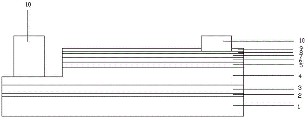
[0021] like figure 1 As shown, the LED chip structure provided by the present invention is efficiently matched with the ZnO thin film, including a substrate 1 and an epitaxial layer formed on the substrate 1, and the epitaxial layer includes a buffer layer 2 grown sequentially, an intrinsic GaN layer 3, Si-doped n-type GaN layer 4, light-emitting multiple quantum well structure 5, electron blocking layer 6, Mg-doped p-type GaN layer 7, contact layer 8 and ZnO transparent conductive layer 9, wherein the buffer layer 2 is GaN Or the AlN buffer layer 2, the n-type GaN layer 4 is provided with an N-type electrode 10, and the Mg-doped P-type GaN layer 7 is provided with a P-type electrode 10.

[0022] During specific implementation, the difference between different embodiments of the present invention mainly lies in the difference of the contact laye...


PUM

PropertyMeasurementUnit
Thicknessaaaaaaaaaa

Abstract

The invention discloses an LED chip structure efficiently matched with a ZnO thin film. The LED chip structure comprises a substrate and an epitaxial layer formed on the substrate. The LED chip structure is characterized in that the epitaxial layer comprises a contact layer and a ZnO transparent conductive layer formed on the contact layer, the contact layer is a superlattice layer composed of a layer of one kind of material or two kinds of materials or three kinds of materials of intrinsic AlxInyGa1-x-yN, P-type AlxInyGa1-x-yN and N-type AlxInyGa1-x-yN. Meanwhile, a manufacturing method of the contact layer is introduced, and the content of the contact layer is achieved by changing the parameters such as In source flow, Al source flow, the growth temperature and the growth pressure. According to the provided ZnO-LED chip structure, the problems such as high voltages, poor ESD and large electric leakage occurring when ZnO serves as the transparent conductive layer are solved, the LED chip structure has the advantages of being good in contact, low in voltage and little in light absorption, and thus the light extraction rate of LED devices is effectively increased.

Description

technical field [0001] The invention relates to the field of manufacturing LED chips, in particular to an LED chip structure with an epitaxial contact layer efficiently matched with a ZnO thin film and a manufacturing method thereof. Background technique [0002] ZnO is a new type of wide-bandgap semiconductor material with high exciton binding energy, and it is an ideal material for light-emitting devices in the future. It has low dielectric constant, high chemical stability, and excellent photoelectric properties. It is a multifunctional material and has very important applications in light-emitting devices, nonlinear optical devices and other fields, and has attracted more and more attention. However, the intrinsic ZnO has n-type conductivity, and it is difficult to achieve P-type doping. Although many domestic and foreign reports have achieved breakthrough results, the current P-line doping is still a key and difficult point for the preparation of ZnO-based light-emitti...

Claims


Application Information

Patent Timeline
IPC IPC(8): H01L33/04H01L33/00
CPCH01L33/06H01L33/0075H01L33/02H01L2933/0008H01L2933/0083
Inventor 罗长得郝锐叶国光许德裕王波易翰翔刘洋吴光芬
Owner GUANGDONG DELI PHOTOELECTRIC
Learn More