Method for forming graphene interconnecting wire

A technology of interconnect wires and graphene, which is applied in the manufacture of electrical components, electrical solid devices, semiconductor/solid devices, etc., can solve the problems of easy damage of graphene films, avoid process risks, avoid transfer processes, and solve easy damage Effect

Active Publication Date: 2015-04-01
SHANGHAI INTEGRATED CIRCUIT RES & DEV CENT
View PDF6 Cites 6 Cited by
  • Summary
  • Abstract
  • Description
  • Claims
  • Application Information

AI Technical Summary

Problems solved by technology

[0006] In view of the above problems, in order to overcome the deficiencies in the prior art, the object of the present invention is to provide a method for forming graphene interconnection lines to solve the problem that graphene films are easily damaged in the prior art

Method used


Image

  • Method for forming graphene interconnecting wire
  • Method for forming graphene interconnecting wire
  • Method for forming graphene interconnecting wire

Examples


Embodiment 1

[0031] see figure 1 , figure 1 It is a schematic flow diagram of a preferred embodiment of a method for forming graphene interconnection provided by the present invention; at the same time, please refer to Figure 2a-2f , Figure 2a-2f It is a structural schematic diagram of a preferred embodiment for forming graphene interconnection provided by the present invention.

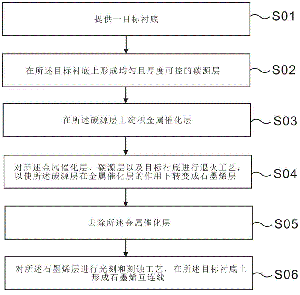
[0032] The present invention provides a method for forming graphene interconnection lines, comprising steps S01 to S06, specifically as follows:

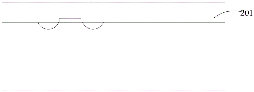
[0033] Such as Figure 2a As shown, step S01: provide a target substrate 201; in this embodiment, the target substrate 201 has completed the preparation of transistor front-end process and via interconnection, and the target substrate 201 includes transistors fabricated on the substrate Included device layers and copper interconnect structures.

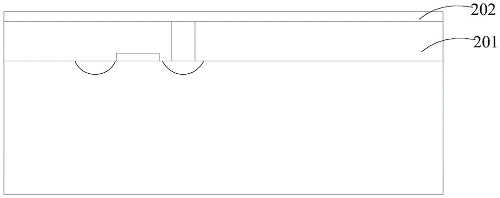
[0034] Such as Figure 2b As shown, step S02: forming a uniform and thickness-controllable carbon source layer 202 o...

Embodiment 2

[0040] In the second embodiment, a method for forming a metal / graphene hybrid interconnection line will be introduced. Please refer to Figure 3a-3f , Figure 3a-3f It is a structural schematic diagram of a preferred embodiment of a method for forming a metal / graphene hybrid interconnection provided by the present invention.

[0041] Different from Embodiment 1, in this embodiment, steps S03 and S05 in Embodiment 1 can be selectively skipped in the method for forming graphene interconnection lines, only steps S01, S02, S04 and S06, specifically Include the following steps:

[0042] Such as Figure 3a As shown in -c, step S01: provide a target substrate 301; specifically, the target substrate 301 has completed the preparation of transistor front-end process and via interconnection, and the target substrate includes transistors fabricated on the substrate. internal device layers and copper interconnect structures. In this embodiment, an intermetallic dielectric layer 302 can ...


PUM

PropertyMeasurementUnit
carrier mobilityaaaaaaaaaa

Abstract

The invention provides a method for forming a graphene interconnecting wire. The method includes the following steps that a target substrate is provided; an even carbon source layer with the adjustable thickness is formed on the target substrate; a metal catalyst layer is deposited on the carbon source layer; then the deposited carbon source layer is converted into a graphene layer at a preset temperature by the adoption of the annealing process; the metal catalyst layer is removed; finally, patterning is carried out on the graphene layer by the adoption of the photoetching process and the etching process, and therefore the graphene interconnecting wire is formed. According to the method for forming the graphene interconnecting wire, the graphene interconnecting wire with the preset thickness can be directly manufactured on the target substrate, an additional graphene transferring process is not needed, and therefore the problem that in the prior art a graphene film is prone to damage is solved; the method is simple and compatible with the traditional CMOS process, and therefore the development and application of the graphene technology are facilitated.

Description

technical field [0001] The invention relates to the technical field of semiconductor integrated circuit manufacturing, and more particularly, to a method for forming graphene interconnection lines. Background technique [0002] In recent years, the rapid development of electronic information industries such as computers, communications, and automation has brought great convenience to people's lives, and the performance of electronic products is getting better and better while they are miniaturized. In this process, single crystal silicon materials have played a huge role, but with the continuous shrinking of device size, limit problems have emerged, such as the reduction of characteristic line width and the limitation of chip integration: on the one hand, it is difficult to continue to achieve The narrower line width is mainly reflected in the problem of lithography accuracy; on the other hand, as the size continues to shrink, some physical effects will affect the normal ope...

Claims


Application Information

Patent Timeline
Patent Type & Authority Applications(China)
IPC IPC(8): H01L21/768
CPCH01L21/76888H01L21/76892H01L2221/1068
Inventor 左青云康晓旭李铭
Owner SHANGHAI INTEGRATED CIRCUIT RES & DEV CENT
Why Eureka
Try Eureka