Printed circuit board and electrocoppering process thereof

A printed circuit board and copper electroplating technology, which is applied in the fields of printed circuit, printed circuit manufacturing, electrical components, etc., can solve the problems of great difficulty in breakthrough and little effect

Active Publication Date: 2015-04-08
GUANGDONG GUANGHUA SCI TECH
View PDF6 Cites 27 Cited by
  • Summary
  • Abstract
  • Description
  • Claims
  • Application Information

AI Technical Summary

Problems solved by technology

However, after years of development and improvement, it is becoming more and more difficult to contin

Method used


Image

  • Printed circuit board and electrocoppering process thereof
  • Printed circuit board and electrocoppering process thereof
  • Printed circuit board and electrocoppering process thereof

Examples


Embodiment 1

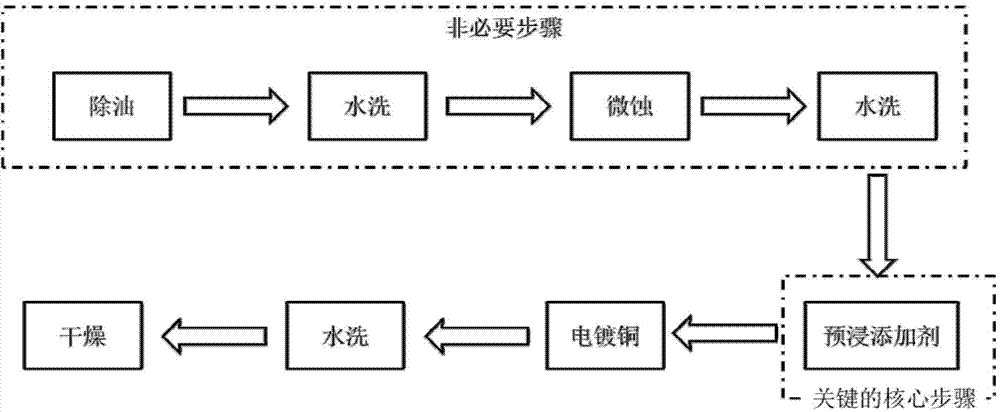
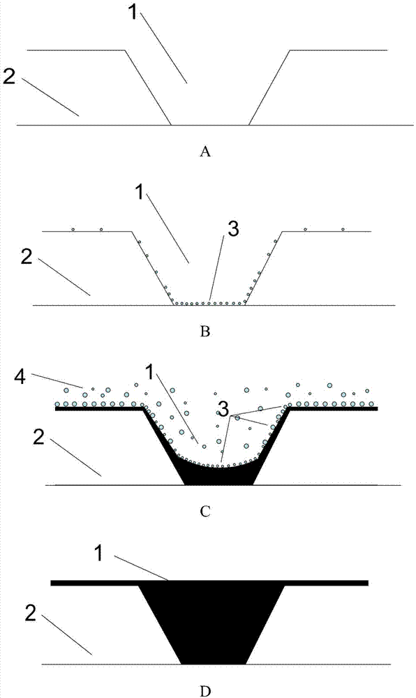
[0059] Use the method of laser ablation to make micro-blind holes with a diameter of 100 μm and an insulating layer thickness of 75 μm. After desmearing, surface adjustment, catalytic activation and electroless copper plating, pre-dip 5% by volume sulfuric acid aqueous solution for 1 min. Put it directly into the electroplating tank for electroplating. The components of the electroplating solution are:

[0060] Copper sulfate pentahydrate: 200g / L

[0061] Sulfuric acid: 60g / L

[0062] Chloride ion: 60mg / L

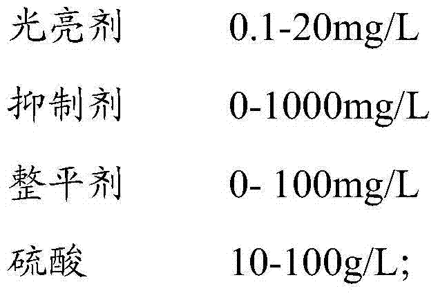
[0063] Hole filling brightener: 0.8mg / L

[0064] Pore ​​filling inhibitor: 30mg / L

[0065] Hole filling and leveling agent: 6mg / L

[0066] Deionized water: balance

[0067] The electroplating current 1.5A / dm 3 , the electroplating temperature is 25°C, turn on the left and right swing and inflate, and the time is 60min. The thickness of the coating and the results of filling blind holes obtained in this embodiment are shown in Table 1.

Embodiment 2

[0069] Use the method of laser ablation to make micro-blind holes with a diameter of 100 μm and an insulating layer thickness of 75 μm. After desmearing, surface adjustment, catalytic activation and electroless copper plating, pre-dip 5% by volume sulfuric acid aqueous solution for 1 min. Then pre-plate a copper layer with a thickness of 5 microns in the pre-plating tank. After one week of storage, take out the plate and go through acid degreasing, cleaning, micro-etching, and then pre-soak 5% sulfuric acid aqueous solution for 1 min, and then directly put it into the electroplating tank. Perform electroplating.

[0070] The components of the pre-plating tank solution are:

[0071] Copper sulfate pentahydrate: 200g / L

[0072] Sulfuric acid: 60g / L

[0073] Chloride ion: 60mg / L

[0074] Pore ​​filling inhibitor: 15mg / L

[0075] Deionized water: balance

[0076] The components of the electroplating solution are:

[0077] Copper sulfate pentahydrate: 200g / L

[0078] Sulfuri...

Embodiment 3

[0086] Use a mechanical numerical control machine to drill a through hole with a diameter of 0.25mm on the printed circuit copper clad substrate. The plate is Shengyi 36 / 1.6FR-4 double-sided copper clad sheet material, and the thickness to diameter ratio of the through hole is 6:1. After desmearing, surface adjustment, catalytic activation and electroless copper plating, it is pre-soaked in 5% by volume sulfuric acid aqueous solution for 1 min, and then directly put into the electroplating tank for electroplating.

[0087] The components of the electroplating solution are:

[0088] Copper sulfate pentahydrate: 70g / L

[0089] Sulfuric acid: 240g / L

[0090] Chloride ion: 60mg / L

[0091] VCP brightener: 0.4mg / L

[0092] VCP inhibitor: 8mg / L

[0093] VCP leveling agent: 2mg / L

[0094] Deionized water: balance

[0095] The electroplating current 3.0A / dm 3 , the electroplating temperature is 25°C, turn on the left and right swing and inflate, and the time is 50min. The analy...


PUM

PropertyMeasurementUnit
Thicknessaaaaaaaaaa
Diameteraaaaaaaaaa
Thicknessaaaaaaaaaa

Abstract

The invention discloses a printed circuit board and an electrocoppering process of the printed circuit board. The printed circuit board comprises a micro blind hole or a micro through hole. The electrocoppering process comprises a pre-treatment step, an electrocoppering step and a post-treatment step. The electrocoppering process is characterized in that a preimpregnation step is further arranged between the pre-treatment step and the electrocoppering step, wherein a first preimpregnation slot and/or a second preimpregnation slot are contained in the preimpregnation step. According to the process disclosed by the invention, high-uniform coatings can be obtained on plating articles with different plate thicknesses/aperture ratios, so that the copper layer uniformity of the through hole of the printed circuit board can be improved, the copper layer thickness of the surface can be effectively reduced, and the TP value can be improved; when the process is applied to filling of the blind hole, the blind hole further can be quickly filled and flattened, so that the electroplating time is shortened and the electroplating copper is saved. The method does not modify existing electrocoppering production line, neither has special requirements on an electroplating additive formula and has very good operability.

Description

technical field [0001] The invention relates to the technical field of printed circuit boards, in particular to a printed circuit board and its copper electroplating process. Background technique [0002] The electroplating copper process is one of the most important processes in the field of PCB manufacturing. The whole process includes the pre-treatment of the board, copper electroplating, and cleaning and drying after electroplating. In the process of making double-sided PCB and multi-layer PCB, the electroplating copper process can be used to thicken the thickness of the copper layer in the micro-via hole, thicken or fill the micro-blind hole, make copper lines, etc., to achieve conduction, interlayer interconnection or Formation of electrical functions such as shielding layer. The electroplated copper layer should be compact, bright and smooth, with good conductivity, good ductility, and high toughness. Therefore, the electroplated copper process is one of the core pro...

Claims


Application Information

Patent Timeline
IPC IPC(8): C25D7/00H05K3/18
Inventor 王翀朱凯程骄肖定军刘彬云何为
Owner GUANGDONG GUANGHUA SCI TECH
Why Eureka
Try Eureka