Wafer cutting device

A cutting device and wafer technology, which is applied to fine working devices, stone processing equipment, manufacturing tools, etc., can solve the problems of easy tool wear, slow etching speed, high consumption, etc., and achieve good processing quality and heat affected zone. Small, high cutting speed

Inactive Publication Date: 2015-04-22
SUZHOU KAIDE MICRO ELECTRONICS CO LTD
View PDF6 Cites 12 Cited by
  • Summary
  • Abstract
  • Description
  • Claims
  • Application Information

AI Technical Summary

Problems solved by technology

Traditional wafer dicing technologies mainly include diamond dicing and chemical etching. The problems of diamond dicing include: wide kerf, low wafer utilization, difficult to process brittle and high-strength materials, easy to produce cracks, fragments and delamin...

Method used


Image

  • Wafer cutting device
  • Wafer cutting device

Examples


Embodiment Construction

[0014] The present invention will be described in further detail in conjunction with the accompanying drawings and specific embodiments.

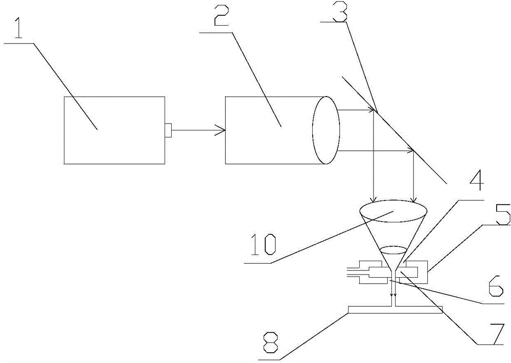
[0015] like figure 1 As shown, the wafer cutting device of the present invention includes a laser 1 , a beam expander 2 , a reflector 3 , a focusing system 10 , a water guide system and a workbench 8 . The wafer to be cut is placed on the workbench 8 , and the laser light generated by the laser 1 enters the focusing system 10 after passing through the beam expander 2 and the reflector 3 .

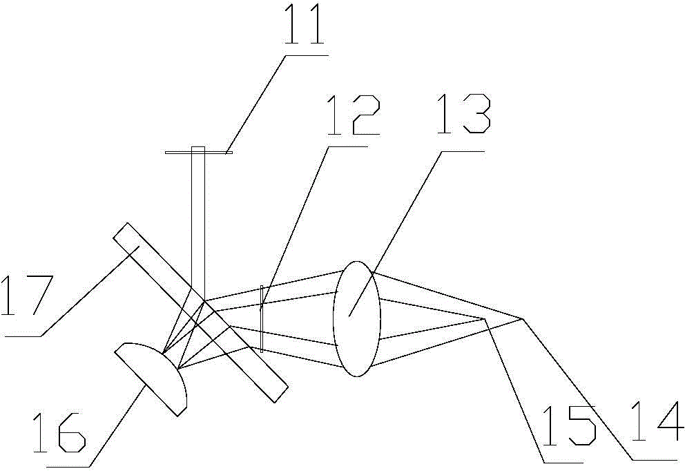
[0016] The focus system of the present invention is a double focus system, such as figure 2 As shown, it is composed of a plano-convex mirror 16, a plane beam splitter 17, a focusing mirror 13, a half-wavelength wave plate 11 and a quarter-wavelength wave plate 12. The laser beam forms parallel light after passing through the mirror and enters the focusing system , in the focusing system, first, the parallel light is converged into one beam through th...


PUM


Abstract

The invention discloses a wafer cutting device. The wafer cutting device comprises a laser, a beam expander, a reflector, a focus system, a water guide system and a worktable, wherein a wafer to be cut is arranged on the worktable, laser light generated by the laser sequentially passes through the beam expander and the reflector and enters the focus system, and focused laser emitted by the focus system is changed into a laser water pillar through the water guide system and emitted onto the worktable for wafer cutting. The focus system is a double-focus system, a front focus and a rear focus are generated on the surface and inside the wafer, the cutting speed is improved, the focused light beam is emitted from a spraying nozzle along with deionized water through the water guide system, the focused laser burns only within the diameter of the water pillar and cuts the wafer, the heat influence is small, the machining quality is improved, and the cutting speed is high.

Description

technical field [0001] The invention relates to a wafer cutting device, which belongs to the technical field of semiconductor processing. Background technique [0002] At present, with the continuous development of silicon wafer chip technology, the integration of chips is getting higher and higher, the size of a single chip is getting smaller and smaller, and the number of chips per unit area is increasing. Efficiency puts new demands on it. Traditional wafer dicing technologies mainly include diamond dicing and chemical etching. The problems of diamond dicing include: wide kerf, low wafer utilization, difficult to process brittle and high-strength materials, easy to produce cracks, fragments and delamination, The tool is easy to wear and needs to consume a lot of deionized water, which increases the cost. The chemical etching method also has some disadvantages, such as slow etching speed, polluting the environment and not being suitable for chemically stable materials. ...

Claims


Application Information

Patent Timeline
IPC IPC(8): B28D5/04
CPCB28D5/04
Inventor 刘思佳
Owner SUZHOU KAIDE MICRO ELECTRONICS CO LTD
Why Eureka
Try Eureka