
High-contrast photonic crystal or, nor and xor logic gate

A photonic crystal, high-contrast technology, applied in logic circuits using optoelectronic devices, logic circuits, logic circuits using specific components, etc. The effect of fast operation

Inactive Publication Date: 2015-04-22
SHENZHEN UNIV
View PDF4 Cites 2 Cited by
  • Summary
  • Abstract
  • Description
  • Claims
  • Application Information

AI Technical Summary

Problems solved by technology

These optical logic devices have the common disadvantage of large volume for the development of large-scale integrated optical circuits
With the improvement of science and technology in recent years, people have also developed quantum optical logic devices, nanomaterial optical logic devices and photonic crystal optical logic devices. These logic devices all meet the size requirements of large-scale photonic integrated optical circuits, but for modern In terms of manufacturing technology, quantum optical logic devices and nanomaterial optical logic devices have great difficulties in manufacturing, while photonic crystal optical logic devices have a competitive advantage in manufacturing technology

Method used


Image

  • High-contrast photonic crystal or, nor and xor logic gate
  • High-contrast photonic crystal or, nor and xor logic gate
  • High-contrast photonic crystal or, nor and xor logic gate

Examples


Embodiment 1

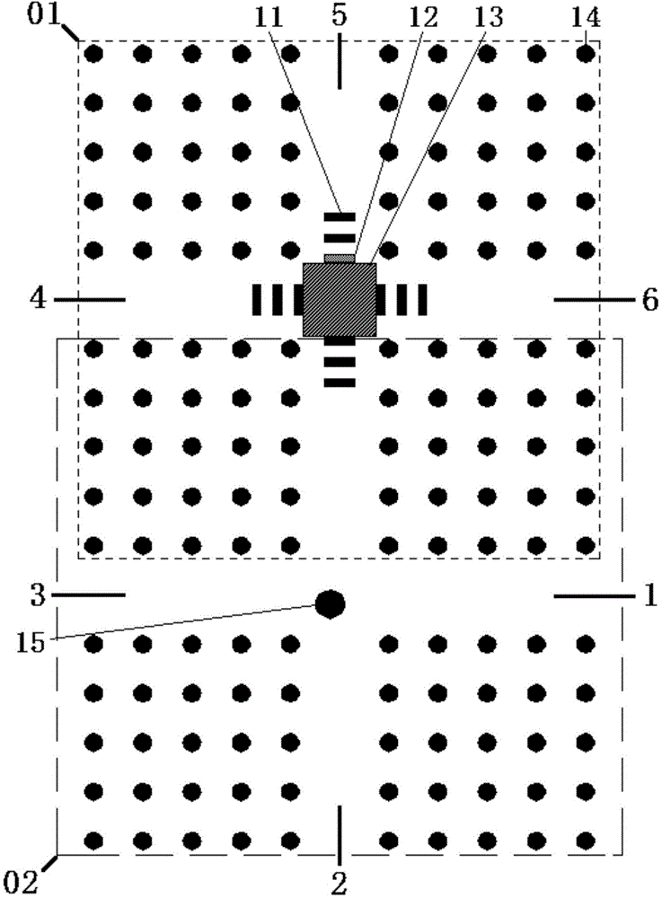
[0064] refer to figure 1 As shown, the lattice constant d=1 μm, the working wavelength is 2.976 μm, the radius of the circular high refractive index linear dielectric column 14 is 0.18 μm; the long side of the first rectangular high refractive index linear dielectric column 11 is 0.613 μm, and the short side is 0.162 μm; the size of the second rectangular high refractive index linear dielectric column 12 is consistent with the size of the first rectangular high refractive index linear dielectric column 11; the side length of the square nonlinear dielectric column 13 is 1.5 μm, and the third-order nonlinear coefficient is 1.33*10 -2 μm 2 / V 2 The distance between two adjacent rectangular linear dielectric columns is 0.2668 μm; the radius of the circular nonlinear dielectric column 15 is 0.292 μm.

[0065] refer to figure 1 As shown in the structure, port 1 and port 4 input reference light E1 and E2 respectively, where E1=E2=1; port 2 input as Figure 5 The Input Signal signa...

Embodiment 2

[0070] refer to figure 1 As shown, the lattice constant d=1 μm, the working wavelength is 2.976 μm, the radius of the circular high refractive index linear dielectric column 14 is 0.18 μm; the long side of the first rectangular high refractive index linear dielectric column 11 is 0.613 μm, and the short side is 0.162 μm; the size of the second rectangular high refractive index linear dielectric column 12 is consistent with the size of the first rectangular high refractive index linear dielectric column 11; the side length of the square nonlinear dielectric column 13 is 1.5 μm, and the third-order nonlinear coefficient is 1.33*10 -2 μm 2 / V 2 The distance between two adjacent rectangular linear dielectric columns is 0.2668 μm; the radius of the circular nonlinear dielectric column 15 is 0.292 μm.

[0071] refer to figure 1 As shown in the structure, port 4 inputs reference light E, E=1; port 1 and port 2 respectively input as Figure 6 The Port1 and Port2 signals shown in ...

Embodiment 3

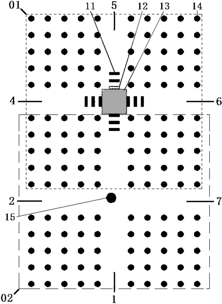
[0077] refer to figure 2 As shown, the lattice constant d=1 μm, the working wavelength is 2.976 μm, the radius of the circular high refractive index linear dielectric column 14 is 0.18 μm; the long side of the first rectangular high refractive index linear dielectric column 11 is 0.613 μm, and the short side is 0.162 μm; the size of the second rectangular high refractive index linear dielectric column 12 is consistent with the size of the first rectangular high refractive index linear dielectric column 11; the side length of the square nonlinear dielectric column 13 is 1.5 μm, and the third-order nonlinear coefficient is 1.33*10 -2 μm 2 / V 2 The distance between two adjacent rectangular linear dielectric pillars is 0.2668 μm; the radius of the circular nonlinear dielectric pillar 15 is 0.292 μm.

[0078] refer to figure 2 As shown in the structure, port 4 inputs reference light E, E=1; port 1 and port 2 respectively input as Figure 7 The Port1 and Port2 signals shown i...


PUM

PropertyMeasurementUnit
refractive indexaaaaaaaaaa

Abstract

The invention discloses a high-contrast photonic crystal or, nor and xor logic gate. The high-contrast photonic crystal or, nor and xor logic gate is a six-port two-dimensional photonic crystal and comprises a nonlinear cavity unit and a cross-shaped waveguide logic gate unit. A high-contrast photonic crystal or logic gate is composed of a reference light input end, two idle light output ends, two system signal input ends and a system signal output end. A high-contrast photonic crystal nor logic gate is composed of two reference light input ends, two idle light output ends, a system signal input end and a system signal output end. A high-contrast photonic crystal xor logic gate is composed of a reference light input end, two idle light output ends, two system signal input ends and a system signal output end. The cross-shaped waveguide logic gate unit is provided with different input or output ports, and the nonlinear cavity unit is connected with the cross-shaped waveguide logic gate unit in a coupled mode. According to the structure, the high-contrast photonic crystal or, nor and xor logic gate and other photonic crystal components are easy to integrate.

Description

technical field [0001] The invention relates to two-dimensional photonic crystals, nonlinear optics, and optical logic gates. Background technique [0002] In 1987, E. Yablonovitch of Bell Laboratories in the United States was discussing how to suppress spontaneous emission, and S. John of Princeton University was discussing the photonic region and independently proposed the concept of photonic crystal (Photonic Crystal). A photonic crystal is a material structure in which dielectric materials are periodically arranged in space, and is usually an artificial crystal composed of two or more materials with different dielectric constants. [0003] With the introduction and in-depth research of photonic crystals, people can more flexibly and effectively control the movement of photons in photonic crystal materials. In combination with traditional semiconductor technology and integrated circuit technology, people are making rapid progress towards all-optical processing through th...

Claims


Application Information

Patent Timeline
Patent Type & Authority Applications(China)
IPC IPC(8): G02F3/00G02F1/35
CPCG02F1/35G02F3/00G02F1/3501G02F1/3511G02B6/1223G02B6/1225G02F1/365G02F2201/06G02F2202/32G02B6/125
Inventor 欧阳征标余铨强
Owner SHENZHEN UNIV
Learn More