Technological method for adjusting barrier height of Schottky diode by doping silicon dioxide film

A technology of Schottky diodes and silicon dioxide films, which is applied in the fields of electrical components, semiconductor/solid-state device manufacturing, circuits, etc., can solve the problems of difficult control of injection uniformity and process repeatability, and few scale applications, so as to achieve centralized distribution , reduce the barrier height, the effect of uniform distribution of impurities

Inactive Publication Date: 2015-04-22
YANGZHOU GUOYU ELECTRONICS
View PDF5 Cites 10 Cited by
  • Summary
  • Abstract
  • Description
  • Claims
  • Application Information

AI Technical Summary

Problems solved by technology

When the number of implanted impurity ions is very small, it is difficult to control the implantation uniformity and process repeatability, and the traditional process method of adjusting the barrier height of Schottky diodes by using an extremely small dose ion implantation process is rarely applied on a large scale

Method used


Image

  • Technological method for adjusting barrier height of Schottky diode by doping silicon dioxide film
  • Technological method for adjusting barrier height of Schottky diode by doping silicon dioxide film
  • Technological method for adjusting barrier height of Schottky diode by doping silicon dioxide film

Examples


Embodiment Construction

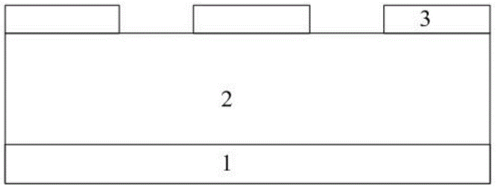
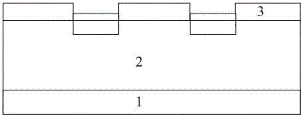
[0023] The process method of adjusting the barrier height of the Schottky diode by doping the silicon dioxide film is made of an N-type single crystal silicon substrate and an N-type single crystal silicon epitaxial layer substrate, and the N-type single crystal on the substrate An oxide layer is formed on the silicon epitaxial layer as a passivation layer, and the thickness of the oxide layer is greater than 400 nanometers; a photolithography and selective etching remove the excess oxide layer to form a doping window; the ion implantation process is used to perform boron doping in the doping window, and at the same time Growth film oxide layer in the doping window forms a P-type protection ring; secondary photolithography and selective etching remove excess oxide layer to form the main surface of the Schottky barrier window; deposit on the main surface of the Schottky barrier window to form a surface The oxide layer of doped silicon dioxide film, the thickness is 50-300 nanome...


PUM


Abstract

A technological method for adjusting the barrier height of a Schottky diode by doping a silicon dioxide film comprises the steps that an N-type single crystal silicon substrate and an N-type single crystal silicon epitaxial layer chip are used as materials, an oxide layer is formed on an N-type single crystal silicon epitaxial layer to be used as a passivation layer, and the thickness of the oxide layer is larger than 400 nanometers; a doping window is formed by primary photoetching; an ion implantation technology is adopted in the doping window for conducting boron doping, and meanwhile the oxide film is grown to form a P-type protecting ring; the main surface of a Schottky barrier window is formed by secondary photoetching; an oxide layer which is doped with the silicon dioxide film and has the surface thickness of 50-300 nanometers is formed on the main surface of the Schottky barrier window in a deposition mode, rapid annealing is conducted under the nitrogen atmosphere to push impurities doped in silicon dioxide towards the N-type single crystal silicon epitaxial layer, and a thin variable doping layer is formed between the oxide layer of the silicon dioxide and the main surface of the N-type epitaxial layer. The barrier height is lowered through the thin variable doping layer.

Description

technical field [0001] The invention relates to the field of manufacturing semiconductor power devices, in particular to a method for manufacturing a Schottky rectifier diode. More specifically, the present invention relates to a process method for adjusting the height of Schottky diode barrier by changing the silicon surface concentration by doping silicon dioxide to form an extremely thin variable doped layer. Background technique [0002] Schottky barrier diodes have low forward voltage drop and high switching speed, and are widely used in low-voltage circuits, but unfortunately, Schottky barrier diodes have a large reverse leakage current at high temperatures, and the reverse leakage The current increases exponentially with temperature, and high temperature power consumption and reliability pose challenges. [0003] In order to solve the problem of high temperature leakage of Schottky barrier diodes, there are currently three main ways, one: increase the barrier height ...

Claims


Application Information

Patent Timeline
Patent Type & Authority Applications(China)
IPC IPC(8): H01L21/329H01L21/205H01L21/324
CPCH01L29/66143H01L21/02532H01L21/02694H01L21/324
Inventor 姚伟明马文力杨勇付国振
Owner YANGZHOU GUOYU ELECTRONICS
Why Eureka
Try Eureka