Preparation method of low-temperature polycrystalline silicon film, TFT, array base plate and display device

A low-temperature polysilicon, amorphous silicon thin film technology, applied in transistors, semiconductor/solid-state device manufacturing, electrical components, etc., can solve problems such as reducing overall electrical performance, unstable threshold voltage, and increasing leakage current

Inactive Publication Date: 2015-04-22
BOE TECH GRP CO LTD
View PDF4 Cites 16 Cited by
  • Summary
  • Abstract
  • Description
  • Claims
  • Application Information

AI Technical Summary

Problems solved by technology

[0005] However, when the amorphous silicon is irradiated by the laser, the temperature generated by the irradiation of each region inside the amorphous silicon is the same, so the growth area of ​​the crystallized polysilicon grains in the LTPS film is random, which makes the LTPS film The grain size is smaller
In this way, when the LTPS film is applied to the active layer of the TFT, when a certain voltage is applied to the gate of the TFT, an electric field will be generated between the gate and the active layer. Under the action of the electric field, the source A conduction state is formed between the electrode and the drain, which is commonly referred to as the channel (channel) when the TFT is turned on. Due to the small grain size of the LTPS, there are more grain boundaries corresponding to the LTPS in the channel, increasing the The leakage current when the TFT is turned on is increased, which leads to the instability of the threshold voltage of the TFT, thereby reducing the overall electrical performance of the TFT

Method used


Image

  • Preparation method of low-temperature polycrystalline silicon film, TFT, array base plate and display device
  • Preparation method of low-temperature polycrystalline silicon film, TFT, array base plate and display device
  • Preparation method of low-temperature polycrystalline silicon film, TFT, array base plate and display device

Examples


preparation example Construction

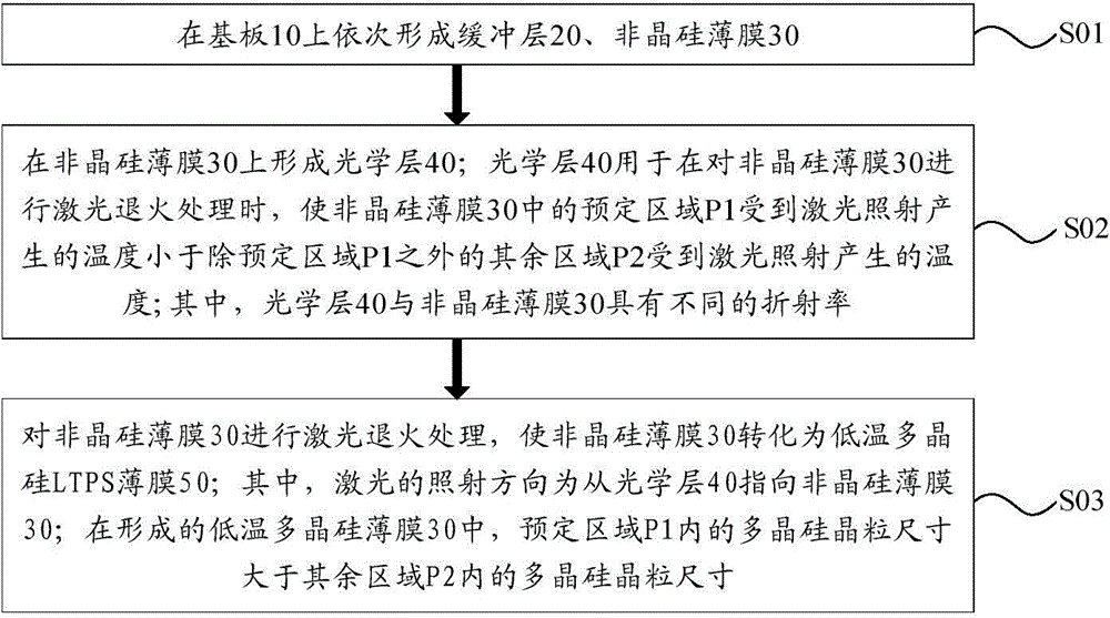
[0035] The embodiment of the present invention provides a method for preparing a low-temperature polysilicon thin film, such as figure 1 As shown, the method includes:

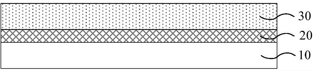
[0036] S01, such as figure 2As shown, a buffer layer 20 and an amorphous silicon thin film 30 are sequentially formed on a substrate 10 .

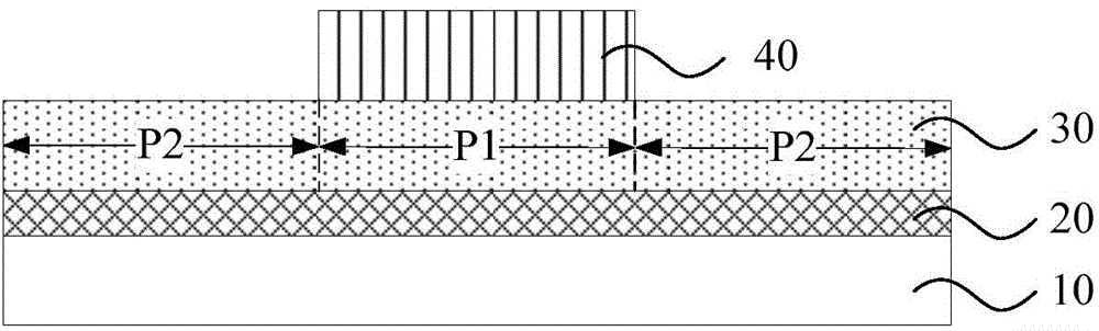
[0037] S02, such as Figure 3A or Figure 3B As shown, an optical layer 40 is formed on the amorphous silicon film 30; the optical layer 40 is used to make the predetermined region in the amorphous silicon film 30 Marked as P1) the temperature produced by laser irradiation is lower than the temperature produced by the rest of the region (marked as P2 in the figure and hereinafter) except the predetermined region P1 by laser irradiation; wherein, the optical layer 40 and the amorphous silicon film 30 have a different refractive indices.

[0038] S03, such as Figure 4A or Figure 4B As shown, the amorphous silicon film 30 is subjected to laser annealing treatment, s...


PUM

PropertyMeasurementUnit
wavelengthaaaaaaaaaa

Abstract

The invention provides a preparation method of a low-temperature polycrystalline silicon film, a TFT, an array base plate and a display device, relates to the technical field of display, and aims at achieving the purposes that an LTPS film prepared by using an ELA method is relatively large in crystal grain size and relatively small in crystal boundary in an area between a source and a drain corresponding to the TFT, the TFT drain current is reduced, and the threshold voltage stability is improved. The preparation method comprises the following steps: forming a buffer layer and an amorphous silicon film; forming an optical layer on the amorphous silicon film, so that the temperature generated when a preset area is radiated by laser is smaller than that generated when other areas are radiated by laser when the amorphous silicon film is subjected to laser annealing treatment; supplying different refractive indexes to the optical layer and the amorphous silicon film; performing laser annealing treatment on the amorphous silicon film so as to convert the amorphous silicon film into a low-temperature polycrystalline silicon film; enabling the size of polycrystalline silicon grains inside the preset area to be greater than that of the polycrystalline silicon grains in other areas. The preparation method is adopted to prepare low-temperature polycrystalline silicon films and thin film transistors with the low-temperature polycrystalline silicon films.

Description

technical field [0001] The invention relates to the field of display technology, in particular to a method for preparing a low-temperature polysilicon thin film, a TFT, an array substrate and a display device. Background technique [0002] Low Temperature Polysilicon (LTPS) thin films have high carrier mobility due to their regular arrangement of atoms (10-300cm 2 / Vs), when applied to thin film transistors (Thin Film Transistor, referred to as TFT) and other electronic components, it can make TFT have a higher driving current. Therefore, LTPS thin film is widely used as one of the core structures of TFT in the manufacturing process of TFT A material for the active layer. [0003] At present, in the preparation process of the TFT, an excimer laser annealing method (Excimer Laser Annealing, ELA for short) is mainly used to form an LTPS thin film. [0004] Among them, the ELA method mainly irradiates the amorphous silicon film with a certain energy excimer laser, and uses th...

Claims


Application Information

Patent Timeline
Patent Type & Authority Applications(China)
IPC IPC(8): H01L21/336H01L21/324H01L21/268H01L29/786H01L29/04
CPCH01L29/6675H01L21/268H01L21/324H01L27/1214H01L29/04H01L29/786
Inventor 左岳平李良坚陈善韬徐文清
Owner BOE TECH GRP CO LTD
Why Eureka
Try Eureka