
Epitaxy structure of InGaN quantum dot and growth method

An epitaxial structure and epitaxial growth technology, applied in electrical components, circuits, semiconductor devices, etc., can solve the problem of restricting the development and application of InGaN quantum dot devices, difficult to obtain high density, high uniformity and high quality InGaN quantum dot materials, Limiting the density of InGaN quantum dots and other issues to achieve the effect of improving device performance, increasing areal density, and reducing threshold current

Active Publication Date: 2015-04-22
INST OF SEMICONDUCTORS - CHINESE ACAD OF SCI
View PDF5 Cites 10 Cited by
  • Summary
  • Abstract
  • Description
  • Claims
  • Application Information

AI Technical Summary

Problems solved by technology

However, the growth of the above-mentioned quantum dots is completely dependent on the distribution of atomic steps on the substrate surface, which limits the further improvement of the density of InGaN quantum dots.
[0004] In summary, the current quantum dot preparation methods are difficult to obtain high-density, high-uniformity and high-quality InGaN quantum dot materials, which seriously restricts the development and application of InGaN quantum dot devices

Method used


Image

  • Epitaxy structure of InGaN quantum dot and growth method
  • Epitaxy structure of InGaN quantum dot and growth method
  • Epitaxy structure of InGaN quantum dot and growth method

Examples


Embodiment Construction

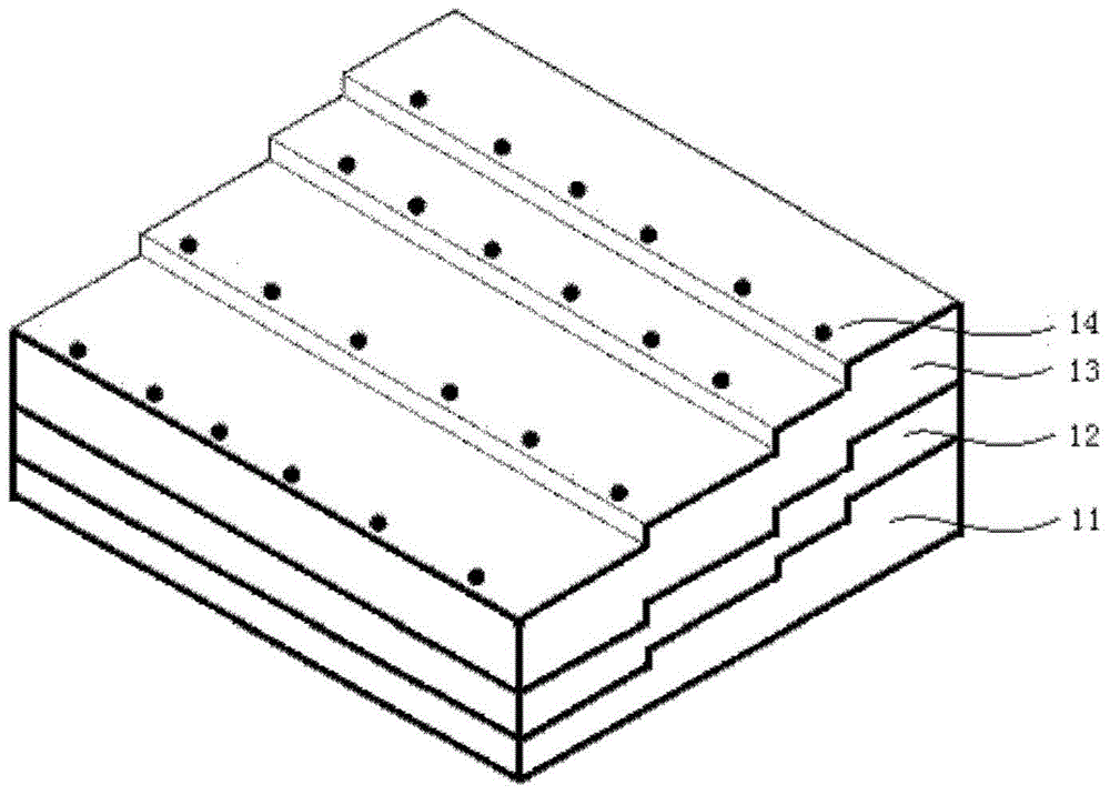
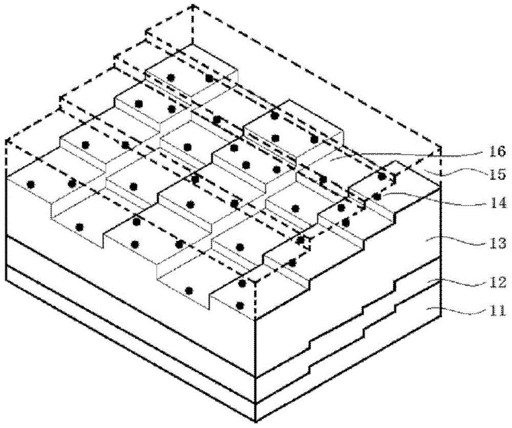
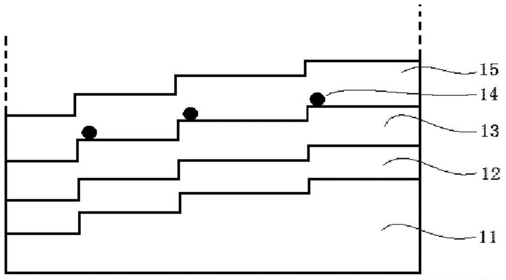
[0029] see figure 2 and image 3 As shown, the epitaxial structure of the InGaN quantum dot provided by the present invention includes:

[0030] A substrate 11, the surface of the substrate 11 has atomic-level step topography, and the bevel angle of the steps is 0.05°-10°. Its material is sapphire, gallium nitride, silicon, silicon carbide or gallium arsenide;

[0031] A low-temperature GaN buffer layer 12 is grown on the substrate 11 . The low-temperature GaN buffer layer 12 has a thickness less than 50 nm and its surface has the same step morphology as that of the substrate 11;

[0032] A high-temperature GaN layer 13 is grown on the low-temperature GaN buffer layer 12 . On its surface, along the direction perpendicular to the steps, uniformly arranged grooves 16 with a depth of 1-100 nm, a width of 10-1000 nm, and a pitch of 0.1-100 μm are etched, so that the surface of the high-temperature GaN layer 13 is staggered and stepped. morphology and form a grid-like structu...


PUM


Abstract

The invention discloses an epitaxy structure of an InGaN quantum dot and a growth method. The epitaxy structure of the InGaN quantum dot comprises a substrate, a low temperature GaN buffering layer, a high temperature GaN layer, a plurality of InGaN quantum dots and a GaN coverage layer, wherein an atomic-scale step form is arranged on the surface of the substrate, and the chamfer angle of steps is 0.05-10 degrees; the low temperature GaN buffering layer is grown on the substrate, and the surface of the low temperature GaN buffering layer is provided with a step form the same as that the substrate; the high temperature GaN layer is grown on the low temperature GaN buffering layer, grooves are etched in the surface of the high temperature GaN layer, the surface of the high temperature GaN layer is of a staggered step form, and a latticed structure is formed on the surface of the high temperature GaN layer; the multiple InGaN quantum dots are distributed and grown on the latticed structure of the surface of the high temperature GaN layer; the GaN coverage layer is grown on the high temperature GaN layer and covers the multiple InGaN quantum dots; the multiple InGaN quantum dots and the GaN coverage layer are sequentially and repeatedly grown on the GaN coverage layer.

Description

technical field [0001] The invention relates to the technical field of semiconductor material growth, in particular to an epitaxial structure and a growth method of high-quality and high-density InGaN quantum dots. The method can be used in the fabrication of active regions of semiconductor optoelectronic devices. Background technique [0002] Traditional InGaN optoelectronic devices use C-plane grown InGaN / GaN multiple quantum well structures. Although the quality of the material grown on the C-plane is high, the strong quantum confinement Stark effect (QCSE) greatly reduces the luminous efficiency of the material, which seriously restricts the improvement of the performance of the light-emitting device. InGaN quantum dots use their special three-dimensional confined structure, which not only reduces the QCSE effect, but also has the advantages of high thermal stability and insensitivity to defects, which can significantly improve the performance of optoelectronic devices....

Claims


Application Information

Patent Timeline
Patent Type & Authority Applications(China)
IPC IPC(8): H01L33/20H01L33/06H01L33/32H01L33/00
CPCH01L33/007H01L33/0075H01L33/06H01L33/20H01L33/32
Inventor 刘炜赵德刚陈平刘宗顺朱建军江德生
Owner INST OF SEMICONDUCTORS - CHINESE ACAD OF SCI
Learn More