Method for forming a film of sensing material in a deep trench

A technology for inductive materials and deep grooves, applied in metal material coating technology, technology for producing decorative surface effects, decorative art, etc., can solve the problem that the semiconductor process steps cannot be carried out, the photoresist cannot be removed cleanly, and the cost is relatively high. Long time and other problems, to achieve the effect of reducing reflectivity, reducing damage to devices, and reducing optical impact

Active Publication Date: 2017-06-06
SHANGHAI HUAHONG GRACE SEMICON MFG CORP
View PDF9 Cites 0 Cited by
  • Summary
  • Abstract
  • Description
  • Claims
  • Application Information

AI Technical Summary

Problems solved by technology

In the degumming step of step 8), chemical acid and alkali solutions cannot be used, and pure oxygen can only be used to ash the photoresist. problems (such as figure 1 , 2 As shown, the photoresist remains after a long time of deglue, because the photoresist and the sensing material are in direct contact, so no matter how much time is ashed, the photoresist cannot be removed), which leads to Subsequent semiconductor process steps cannot be performed

Method used


Image

  • Method for forming a film of sensing material in a deep trench
  • Method for forming a film of sensing material in a deep trench
  • Method for forming a film of sensing material in a deep trench

Examples


Embodiment Construction

[0037] In order to have a more specific understanding of the technical content, characteristics and effects of the present invention, now in conjunction with the accompanying drawings, the present invention is described in detail as follows:

[0038] The method for forming an inductive material film in a deep groove of the present invention has a specific process flow as follows:

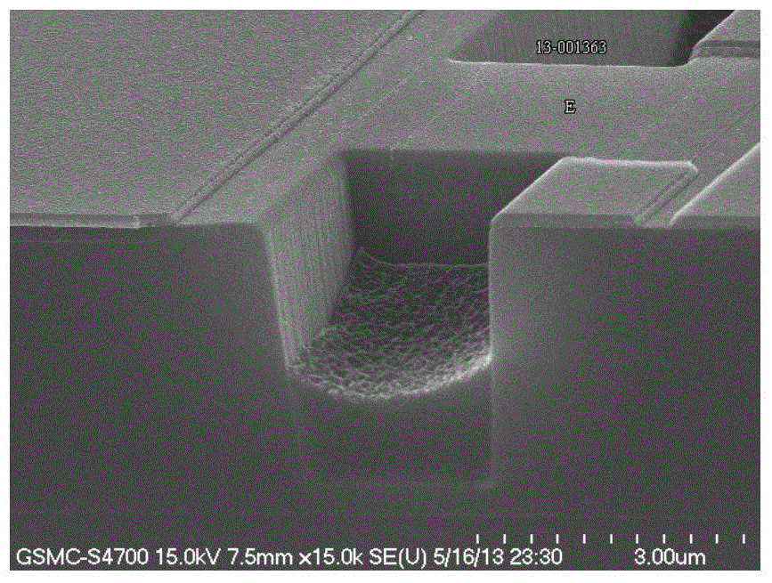
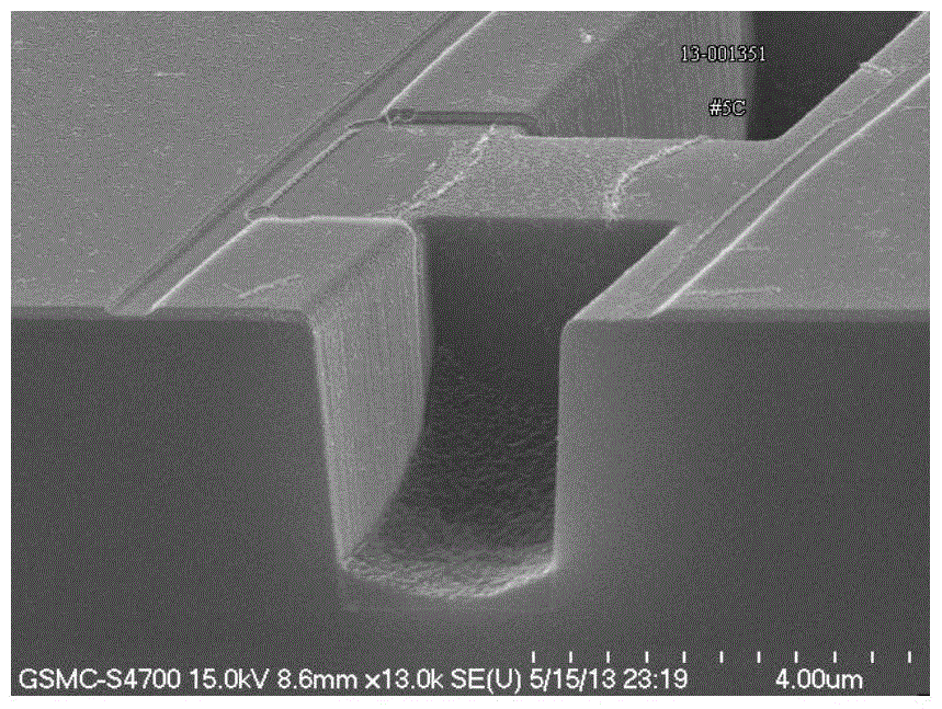
[0039] Step 1, grow a layer of hard mask 102 on the silicon substrate 101, such as image 3 shown. The material of the hard mask 102 may be silicon oxide or silicon nitride.

[0040] Step 2, coating a layer of photoresist 103, and forming a deep trench photolithographic window, such as Figure 4 shown.

[0041] The photoresist 103 can be positive or negative, and the photoresist used in this embodiment is TOK P6159. A typical baking temperature is 90°C for 60 seconds. The lithography machine can use any type of lithography machine, and the typical lithography machine is Nikon I-14.

[0042] St...


PUM

PropertyMeasurementUnit
thicknessaaaaaaaaaa
thicknessaaaaaaaaaa
thicknessaaaaaaaaaa

Abstract

The invention discloses a method for forming an induction material membrane in a deep groove. The method comprises steps as follows: 1) growing a hard mask layer on the surface of a silicon substrate; 2) coating the hard mask layer with a photoresist, and forming a deep groove photolithographic window; 3) forming the deep groove through photolithographic etching, and then removing the photoresist; 4) performing wet etching, and removing the hard mask layer; 5) depositing an induction material; 6) depositing a silicon oxynitride anti-reflection layer; 7) applying an organic anti-reflection layer; 8) applying the photoresist; 9) performing exposure development and etching to form a final pattern; 10) removing the photoresist and the organic anti-reflection layer. On the basis of an existing technology, the membrane layer structure is optimized, so that the photoresist can be very easily and effectively removed in a follow-up process and is prevented from remaining, and meanwhile, the photoresist removal cost and damage to devices are reduced.

Description

technical field [0001] The invention relates to the field of integrated circuit manufacturing, in particular to a method for forming an inductive material film in a deep groove. Background technique [0002] Micro-Electro-Mechanical Systems (MEMS) is a multidisciplinary frontier research field developed on the basis of microelectronics technology. As far as the semiconductor industry is concerned, the integration of MEMS and production process technology will bring a great leap forward for the system single chip. In the future, it is expected to integrate subsystems such as audio, light, chemical analysis, pressure, and temperature sensing in a single chip, and develop chips with sensory functions such as human eyes, nose, ears, and skin; The ability to control is beyond the ability of the human body. [0003] At present, there are three main technologies commonly used to manufacture MEMS devices: [0004] The first is the method of using traditional mechanical processing...

Claims


Application Information

Patent Timeline
Patent Type & Authority Patents(China)
IPC IPC(8): B81C1/00
Inventor 孟鸿林时挺
Owner SHANGHAI HUAHONG GRACE SEMICON MFG CORP
Why Eureka
Try Eureka