Eureka AIR delivers breakthrough ideas for toughest innovation challenges, trusted by R&D personnel around the world.

Substrate transferring method for power semiconductor device with perpendicular structure

A technology for power semiconductor and substrate transfer, applied in the fields of semiconductor devices, semiconductor/solid-state device manufacturing, electric solid-state devices, etc., can solve the problems of short circuit, inability to manufacture vertical structure devices, device failure, etc., achieving low consumption and easy implementation , to ensure the effectiveness of the effect

Inactive Publication Date: 2015-04-29
JIANGSU CORENERGY SEMICON CO LTD
View PDF5 Cites 14 Cited by
  • Summary
  • Abstract
  • Description
  • Claims
  • Application Information

AI Technical Summary

Problems solved by technology

Therefore, most processes generally use sapphire as the substrate, but the sapphire substrate also has the following defects: sapphire is an insulator, and its resistivity at room temperature is greater than 1011Ω·cm. In this case, it is impossible to fabricate devices with vertical structures. Usually only n-type and p-type electrodes are made on the upper surface of the epitaxial layer
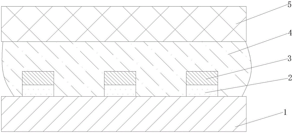
However, the following problems usually exist during operation, see figure 1 As shown, during the bonding process, the solder contacts the metal electrode and the epitaxial layer, resulting in short circuit and device failure.
At present, researchers do not have a good solution to solve this problem

Method used


Image

  • Substrate transferring method for power semiconductor device with perpendicular structure
  • Substrate transferring method for power semiconductor device with perpendicular structure
  • Substrate transferring method for power semiconductor device with perpendicular structure

Examples


Embodiment Construction

[0027] The technical solution of the present invention will be further described below in conjunction with the accompanying drawings.

[0028] see Figure 2-9 As shown, a substrate transfer method for a vertical structure power semiconductor device, the power semiconductor device arranged on the sapphire substrate 1 is transferred to the target substrate 5, and the power semiconductor device includes epitaxial growth on the sapphire substrate 1 Layer 2 and a plurality of metal electrode blocks 3 that are plated on the upper surface of the epitaxial layer 2 at intervals, the substrate transfer method mainly includes the following steps:

[0029] 1) Place solder 4: place solder 4 as a bonding material on the upper surface of the metal electrode block of the power semiconductor device, the projected area of ​​the solder 4 on the horizontal plane is smaller than the projected area of ​​the metal electrode block 3 on the horizontal plane;

[0030] 2) Wafer bonding: the tar...


PUM


Abstract

The invention discloses a substrate transferring method for a power semiconductor device with perpendicular structure. The power semiconductor device arranged on a sapphire substrate is transferred to a target substrate and comprises extension layers growing on the sapphire substrate and a plurality of metal electrode blocks plated on the upper surfaces of the extension layers. The substrate transferring method mainly comprises the following steps: 1, placing a welding flux, namely, placing the welding flux on the surface of the power semiconductor device; 2, bonding a wafer, namely, bonding the upper surface of the power semiconductor device to the target substrate through the welding flux by a wafer bonding technology; 3, peeling the sapphire substrate, namely, peeling the sapphire substrate from the power semiconductor device by a laser peeling technology to finish the transferring of the power semiconductor device. The method is simple to operate and can effectively prevent device short-circuiting and failure conditions due to the simultaneous contact of the welding flux with the metal electrode blocks and the extension layers of the device which is caused by excessive welding flux placed when the device is bonded with the target substrate.

Description

technical field [0001] The invention relates to a substrate transfer method of a vertical structure power semiconductor device, belonging to the technical field of semiconductor technology. Background technique [0002] At present, sapphire, silicon, and silicon carbide are generally used as substrates to grow epitaxial layers in semiconductor processes. Generally, the epitaxial layer of GaN-based materials and devices is mainly grown on sapphire substrates. Sapphire substrates have many advantages: 1. The production technology of sapphire substrates is mature and the quality of devices is good; 2. Sapphire has good stability and can be used During the high temperature growth process; 3. Sapphire has high mechanical strength and is easy to handle and clean. Therefore, most processes generally use sapphire as the substrate, but the sapphire substrate also has the following defects: sapphire is an insulator, and its resistivity at room temperature is greater than 1011Ω·cm. ...

Claims


Application Information

Patent Timeline
IPC IPC(8): H01L21/50H01L21/60
CPCH01L21/50H01L24/81H01L2224/81192
Inventor 苗操伊迪亚·乔德瑞杨秀程朱廷刚艾俊王科
Owner JIANGSU CORENERGY SEMICON CO LTD
Why Eureka
Eureka Blog
Learn More