High-speed avalanche photodetector chip with carrier and manufacturing method thereof

A detector chip, avalanche photoelectric technology, applied in the field of optical transmission network, can solve the problems of low chip coupling efficiency, difficult to achieve receiving sensitivity, reduced capacitance and chip distribution parameters, etc., to improve the chip transmission rate, reduce the overall distribution parameters, The effect of improving the reception sensitivity

Active Publication Date: 2016-06-15
SHENZHEN PHOGRAIN INT TECH DEV
View PDF6 Cites 0 Cited by
  • Summary
  • Abstract
  • Description
  • Claims
  • Application Information

AI Technical Summary

Problems solved by technology

In this structure, in order to increase the transmission rate of the APD chip, the thickness D1 of the absorption layer 300 is usually reduced to less than 1um to achieve the purpose of shortening the transit time of photogenerated carriers; and at the same time, the Zn diffusion diameter of the light absorption region 800 D2 is reduced to less than 20um. This design structure can usually make the APD chip meet the requirements of 10G transmission rate, but there are the following problems: 1. Because the thickness of the InGaAs absorbing layer 300 is too thin, resulting in low photoresponsivity, the design structure made The receiving sensitivity of the 10GAPD chip is difficult to meet the application requirements of -26dBm; 2. Because the absorption diameter of the light absorption area 800 is too small, the coupling efficiency of the chip is extremely low, and it is difficult to meet the production and use requirements
However, in order to meet the requirement of high bandwidth, it is still necessary to reduce the Zn diffusion diameter D2 of the light absorption region 800 to less than 20um, so the APD chip of this method still has the problem of low coupling efficiency and it is difficult to meet the use requirements.
At present, the third approach is to use InAlAs superlattice and mesa structure to realize together, such as image 3 As shown, different from the APD chip with the traditional InGaAs / InP / InGaAsP structure, the multiplication layer of the APD chip with this structure is mainly composed of the superlattice 204 composed of AlInAs / AlGaInAs, because AlInAs has a higher electron space than the traditional InP material Cave ionization coefficient ratio, so the APD chip with this structure has a high multiplier response, and because of the mesa structure design, the capacitance and chip distribution parameters of the chip have been reduced, which can meet the requirements of 10G optical transmission network. However, the APD chip with this structure also has a difficult manufacturing process. The AlInAs / AlGaInAs superlattice structure requires the thickness of each layer to be accurately controlled to less than 1nm, which is difficult to achieve for the usual manufacturing process.
In addition, due to the mesa structure used in this structure, there is also a certain reliability risk in the long-term reliability of the chip
Therefore, there is still a lack of a high-speed APD chip for 10G optical transmission networks that is truly practical and can be mass-produced with excellent performance.

Method used


Image

  • High-speed avalanche photodetector chip with carrier and manufacturing method thereof
  • High-speed avalanche photodetector chip with carrier and manufacturing method thereof
  • High-speed avalanche photodetector chip with carrier and manufacturing method thereof

Examples


Embodiment Construction

[0031] The present invention will be described in detail below in conjunction with the accompanying drawings and specific embodiments.

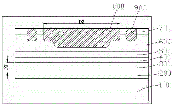
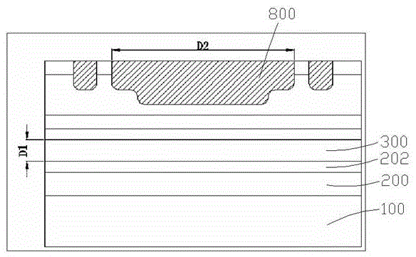
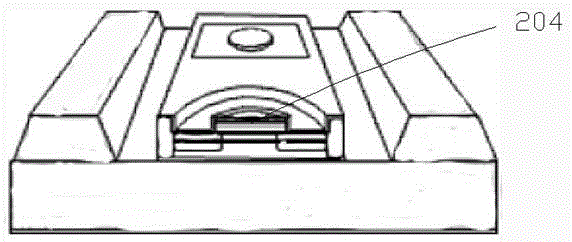
[0032] see Figure 4 to Figure 7 , the present invention provides a high-speed avalanche photodetector chip with a carrier, which is mainly composed of three parts, specifically including: a carrier 13, several solder balls 12 welded on the carrier 13, and soldered to the carrier in a flip-chip manner. The epitaxial wafer 40 on several welding balls 12, the carrier 13 is a ceramic carrier, and a metal pattern is formed on its surface, and the radius R1 of the welding ball 12 is greater than 10um and less than 50um, which can ensure that after welding, the epitaxial wafer 40 and The distance D3 between the carriers 13 is larger than 10um. The epitaxial wafer 40 includes: a substrate 18, a buffer layer 19 formed on the substrate 18, an absorption layer 20 formed on the buffer layer 19, a transition layer 21 formed on the absorption layer 20, ...


PUM


Abstract

The invention discloses a high-speed avalanche photodetector chip with a carrier and a manufacturing method for the high-speed avalanche photodetector chip. The high-speed avalanche photodetector chip comprises the carrier, a plurality of welding balls welded on the carrier and an epitaxial wafer inversely welded on the welding balls, wherein the epitaxial wafer comprises a substrate, a buffer layer formed on the substrate, an absorption layer formed on the buffer layer, a transition layer formed on the absorption layer, a field control layer formed on the transition layer, a top layer formed on the field control layer, a contact layer formed on the top layer, a diffusion region formed in the top layer and the contact layer, a positive electrode formed on the diffusion region, a negative electrode formed on the contact layer and the buffer layer, a micro-lens formed at the bottom of the substrate, and an antireflection film formed on the surface of the micro-lens; the positive electrode and the negative electrode are welded on the welding balls; the diffusion region comprises a diffusion multiplication region and a diffusion protection ring which are concentric; the radius of the diffusion multiplication region is greater than 15 microns and smaller than 30 microns.

Description

technical field [0001] The invention relates to the technical field of optical transmission networks, in particular to a high-speed avalanche photodetector chip with a carrier and a manufacturing method thereof. Background technique [0002] In the optical network transmission system, since there is always a certain loss in the transmission of light in the optical fiber, at the receiving end of the optical transmission system, in order to capture the weak optical signal of the optical transmission terminal, an avalanche with signal amplification function is often used The photodetector chip, that is, the APD chip, especially in the long-distance optical transmission system, the APD chip is an indispensable key chip. In addition, with the continuous improvement of optical transmission rate, 10G optical transmission network has been rolled out in a large number, and the rate of the receiving chip required to be applied is also continuously increasing. The usual 2.5GAPD chip ca...

Claims


Application Information

Patent Timeline
Patent Type & Authority Patents(China)
IPC IPC(8): H01L31/107H01L31/0352H01L31/0232H01L31/18
CPCH01L31/0232H01L31/0352H01L31/107H01L31/184Y02P70/50
Inventor 王建
Owner SHENZHEN PHOGRAIN INT TECH DEV
Why Eureka
Try Eureka