Laser cutting method for high-power power electronic device wafer

A power electronic device, laser cutting technology, applied in the direction of electrical components, laser welding equipment, semiconductor/solid-state device manufacturing, etc., can solve problems such as thinning difficulties, reduce chip damage, optimize depth and width, reliability and production capacity Enhanced effect

Active Publication Date: 2015-05-06
STATE GRID CORP OF CHINA +1
View PDF3 Cites 11 Cited by
  • Summary
  • Abstract
  • Description
  • Claims
  • Application Information

AI Technical Summary

Problems solved by technology

[0005] In order to solve the existing problems of laser cutting, the laser cutting of high-power power electronic device wafers is mainly improved, considerin

Method used


Image

  • Laser cutting method for high-power power electronic device wafer
  • Laser cutting method for high-power power electronic device wafer
  • Laser cutting method for high-power power electronic device wafer

Examples


Embodiment 1

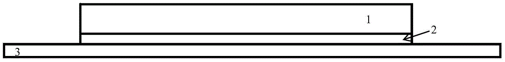
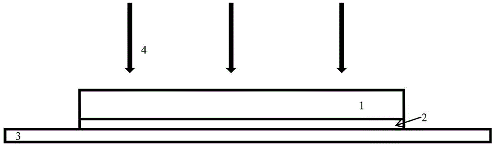
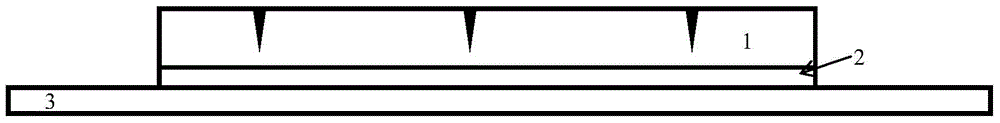
[0053] Under the guidance of the cutting principle provided by the present invention, the specific implementation parameters are selected: laser beam wavelength is 248nm, cutting groove depth is 20μm, groove width is 12μm, laser beam power is 5W, focusing distance is 400μm, and laser cutting speed is 10mm / s.

Embodiment 2

[0055] Under the guidance of the cutting principle provided by the present invention, specific implementation parameter selection: laser beam wavelength 190nm, cutting groove depth 15μm, groove width 10μm, laser beam power 10W, focusing distance 330μm, laser cutting speed 10mm / s.

Embodiment 3

[0057] Under the guidance of the cutting principle provided by the present invention, the specific implementation parameters are selected: laser beam wavelength is 400nm, cutting groove depth is 35μm, groove width is 8μm, laser beam power is 8W, focusing distance is 400μm, and laser cutting speed is 20mm / s.


PUM

PropertyMeasurementUnit
Wavelengthaaaaaaaaaa
Poweraaaaaaaaaa

Abstract

The invention discloses a cutting method for a high-power power electronic device chip. The cutting method for the high-power power electronic device chip includes that carrying out laser scribing on the back of a substrate of a device made of wide band-gap semiconductor material, and using a breaker to break the front according to the back scratch. The depth of the back scratch is about 1/10 to 1/4 of the chip thickness. The cutting method for the high-power power electronic device chip uses a laser beam focusing cutting method, the laser beam cuts the high-power device through back scribing, an active region at the front of the chip is greatly guaranteed, the front region is not damaged, the edges of the device are regular, and the reliability and yield of the large-area chip are greatly improved.

Description

【Technical field】 [0001] The invention relates to a semiconductor power device preparation process, in particular to a process for dividing a high-power device wafer into single chips during the preparation process of a high-power power electronic device. 【Background technique】 [0002] With the rapid development of the optoelectronic industry, the demand for highly integrated and high-performance semiconductor wafers is also increasing. The third-generation semiconductor developed to adapt to special environments such as high frequency, high power, high temperature resistance, and radiation resistance. Materials-Wide bandgap semiconductor materials (such as silicon carbide, gallium nitride, etc.) have the characteristics of high thermal conductivity, high electron saturation velocity, high breakdown voltage, and low dielectric constant, which opens up a new situation in the semiconductor industry and makes Power electronic device technology and industry ushered in a new opp...

Claims


Application Information

Patent Timeline
IPC IPC(8): H01L21/268H01L21/78
CPCB23K26/38H01L21/268H01L21/78
Inventor 田亮杨霏
Owner STATE GRID CORP OF CHINA
Why Eureka
Try Eureka