Tunneling field effect transistor and forming method thereof

A tunneling field effect and transistor technology, which is applied in semiconductor devices, semiconductor/solid-state device manufacturing, electrical components, etc., can solve the problem of leakage current damage to sub-threshold swings, difficulty in realizing narrow tunneling junctions, and difficulty in turning off devices, etc. problems, to achieve the effect of improving sub-threshold characteristics, reducing leakage current, and increasing conduction current

Active Publication Date: 2015-05-06
INST OF MICROELECTRONICS CHINESE ACAD OF SCI
View PDF4 Cites 2 Cited by
  • Summary
  • Abstract
  • Description
  • Claims
  • Application Information

AI Technical Summary

Problems solved by technology

However, in order to reduce the sub-threshold swing and increase the conduction current, the tunneling junction needs to be as narrow as possible. However, the tunneling field effect transistor with the existing structure will always cause the diffusion distribution of impurities during the injection and heat treatment process, and it is difficult to achieve a narrow tunneling junction. tunneling junction
[0005] In addition, in conventional tunneling field effect transistors, the source and drain regions are highly doped, and the doping will inevitably introduce defects, and the leakage current associated with these defects will destroy the reduction of the subthreshold swing.
Moreover, conventional tunneling field effect transistors have bipolar characteristics that can be turned on at both positive and negative gate voltages, making it difficult to completely turn off the device

Method used


Image

  • Tunneling field effect transistor and forming method thereof
  • Tunneling field effect transistor and forming method thereof
  • Tunneling field effect transistor and forming method thereof

Examples


Embodiment 1

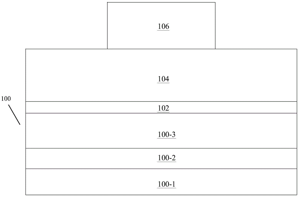
[0060] First, in step S101, an SOI substrate 100 is provided, referring to figure 1 shown.

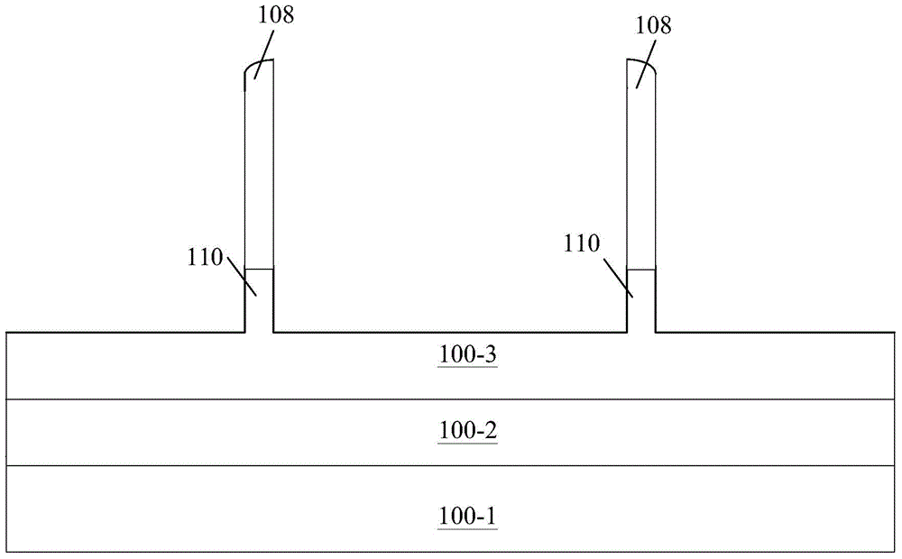
[0061] The SOI substrate 100 is composed of the bottom silicon 100-1, the buried oxide layer 100-2 and the top silicon 100-3, and the fins are formed by the top silicon 100-3.

[0062] Next, in step S102 , the fins 110 are formed.

[0063] In the present invention, the width of the tunnel junction is controlled by the width of the fin. Of course, the narrower the tunnel junction, the better. The method proposed in this embodiment is especially suitable for the formation of narrow fins, for example, the width is about 10nm or narrower. the fins.

[0064] In this embodiment, the following steps are specifically included:

[0065] First, a silicon oxide layer 102 and a polysilicon layer 104 are sequentially deposited on a semiconductor substrate, and a photosensitive etchant 106 is formed on the polysilicon layer 104, such as figure 1 shown.

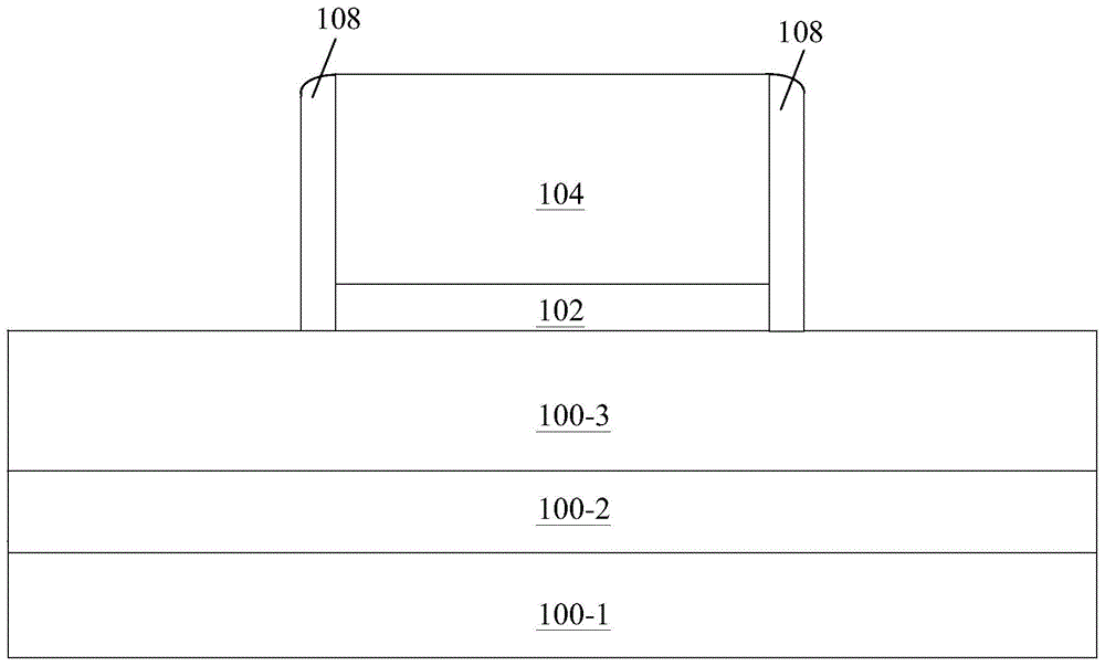
[0066] Next, etching is performed usin...

Embodiment 2

[0085] First, in step S201, an SOI substrate 200 is provided, referring to Figure 15 shown.

[0086] The SOI substrate 200 is composed of bottom silicon 200-1, buried oxide layer 200-2 and top silicon 200-3, and the fins are formed by top silicon 200-3.

[0087] Then, in step S202, a silicon oxide layer 202 and a polysilicon layer 204 are sequentially deposited on the semiconductor substrate, and a photosensitive etchant 206 is formed on the polysilicon layer 204, such as Figure 15 shown.

[0088] Next, in step S203, the polysilicon layer 204 is etched to form a patterned polysilicon layer 204, and a fin capping layer 214 is formed on the sidewall of the polysilicon layer 204, and a first gate capping layer is formed on the sidewall of the fin capping layer 214 212, such as Figure 16 shown.

[0089] In this embodiment, the fin capping layer 214 is silicon nitride with a width of less than 10 nm, the first gate capping layer 212 is SiGe, and the polysilicon layer 204 is ...


PUM


Abstract

The invention provides a tunneling field effect transistor comprising a semiconductor substrate, first gates, second gates, first doped regions, and second doped regions. Fins are formed on the semiconductor substrate. Each first gate and the corresponding second gate are respectively formed on the semiconductor substrate at the two sides of the corresponding fin. A gate dielectric layer is formed among each first gate, a first side of the corresponding fin and the semiconductor substrate, and a gate dielectric layer is formed among each second gate, a second side of the corresponding fin and the semiconductor substrate. The first doped regions and the second doped regions are respectively disposed in the semiconductor substrate at one side of the first gates and at one side of the second gates. A narrow tunneling junction is realized by controlling the width of the fins, the tunneling current is increased, and the conduction current is further improved by increasing the effective tunneling area. In addition, defect-related leakage current can be inhibited, and the sub threshold characteristic of devices can be improved.

Description

technical field [0001] The invention relates to the field of semiconductor devices, in particular to a tunneling field effect transistor and a forming method thereof. Background technique [0002] With the continuous shrinking of the device size, the number of devices per unit area of ​​the chip is increasing, and how to reduce power consumption has become an increasingly prominent problem. [0003] The structure of a conventional tunneling field effect transistor (conventional-TFET) mainly includes a substrate (channel), a gate dielectric layer, a gate, and source / drain regions on both sides of the gate. It mainly works based on the quantum tunneling effect. Taking the P-type tunneling field effect transistor as an example, a negative voltage is applied to the gate, the potential of the channel region rises, quantum tunneling occurs from the source region to the channel region, and the electrons and holes generated by the tunneling pass from the source region to the channel...

Claims


Application Information

Patent Timeline
Patent Type & Authority Applications(China)
IPC IPC(8): H01L29/78H01L29/08H01L21/336
CPCH01L29/0847H01L29/66484H01L29/66795H01L29/7855
Inventor 朱正勇朱慧珑许淼
Owner INST OF MICROELECTRONICS CHINESE ACAD OF SCI
Why Eureka
Try Eureka