Manufacturing method of hetero-junction solar cell and hetero-junction solar cell

A technology of solar cells and manufacturing methods, applied in the direction of final product manufacturing, sustainable manufacturing/processing, circuits, etc., can solve the problems of inability to reduce battery efficiency loss, decrease battery conversion efficiency, increase battery series resistance, etc., and achieve improved Photoelectric conversion efficiency and the effect of improving battery performance

Inactive Publication Date: 2015-05-06
APOLLO PRECISION (FUJIAN) LIMITED
View PDF2 Cites 8 Cited by
  • Summary
  • Abstract
  • Description
  • Claims
  • Application Information

AI Technical Summary

Problems solved by technology

However, the thickness of the intrinsic amorphous silicon layer is an important factor affecting the performance of the HIT battery. On the one hand, due to the low conductivity of the intrinsic amorphous silicon layer itself, too thick an intrinsic amorphous silicon layer will increase the performance of the battery. Connecting resistors in series reduces the filling factor accordingly, thereby reducing the conversion efficiency of the battery; in order to make the crystalline silicon have a good light-trapping effect, it is necessary to carry out texturing treatment on the crystalline silicon, because the surface roughness of the crystalline silicon

Method used


Image

  • Manufacturing method of hetero-junction solar cell and hetero-junction solar cell
  • Manufacturing method of hetero-junction solar cell and hetero-junction solar cell
  • Manufacturing method of hetero-junction solar cell and hetero-junction solar cell

Examples


no. 1 example

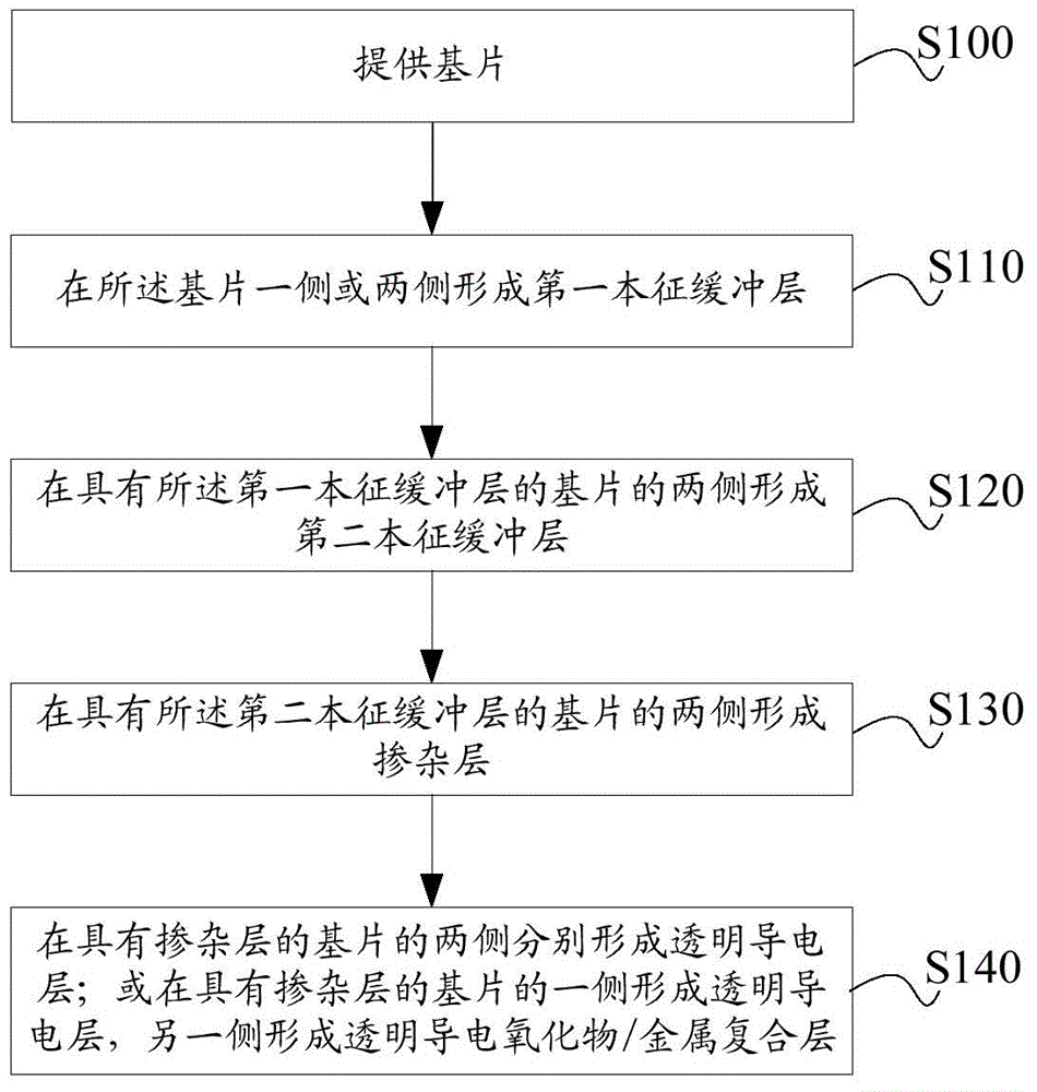
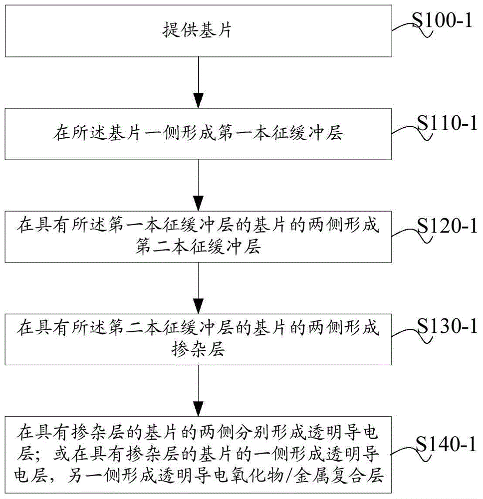
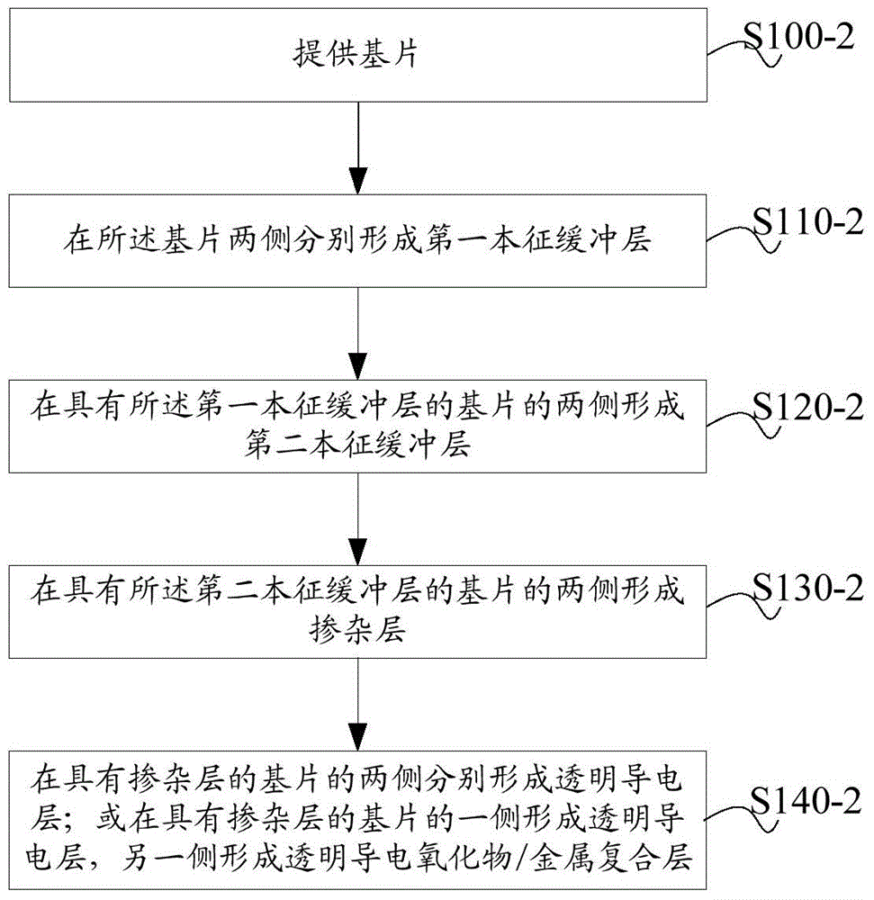
[0039] Please refer to figure 2 as shown, figure 2 It is a flow chart of the first embodiment of a method for manufacturing a heterojunction solar cell provided by the present application; this embodiment specifically includes the following steps:

[0040] Step S100-1: providing a substrate;

[0041] The substrate is made of a crystalline silicon material, which can be a monocrystalline silicon body or a polycrystalline silicon body. In this embodiment, an N-type monocrystalline silicon wafer can be selected, and its thickness range is greater than or equal to 150um and less than or equal to 300um, preferably It is 180um and the resistivity is 3Ωcm. For silicon wafers, it needs to be textured and cleaned first. The purpose of texturing is to reduce the reflection of the battery surface so that more photons can be absorbed by the substrate. Usually, the surface of silicon wafers is treated into a pyramid shape. The shape is more conducive to the oblique incidence of light ...


PUM

PropertyMeasurementUnit
Thickness rangeaaaaaaaaaa

Abstract

The invention discloses a manufacturing method of a hetero-junction solar cell. The manufacturing method of the hetero-junction solar cell comprises the steps that a substrate is provided; first intrinsic buffer layers are formed on one side or two sides of the substrate; second intrinsic buffer layers are formed on the two sides of the substrate with the first intrinsic buffer layers; doping layers, namely the first doping layer and the second doping layer, are formed on the two sides of the substrate with the second intrinsic buffer layers; transparent conducting layers are formed on the two sides of the substrate with the doping layers; or a transparent conducting layer is formed on one side of the substrate with the doping layers, and a transparent conducting oxide/metal composite layer is formed on the other side of the substrate with the doping layers. Therefore, the photoelectric conversion efficiency of the hetero-junction solar cell is improved. In addition, the invention provides the hetero-junction solar cell.

Description

technical field [0001] The present application relates to the field of new energy, in particular to a method for manufacturing a heterojunction solar cell and the heterojunction solar cell. Background technique [0002] Solar cells can also be called photovoltaic cells, which is a new power generation technology that uses the photovoltaic effect to directly convert solar radiation into electrical energy. Because of its abundant raw materials, cleanliness, safety, and long life, it is considered to be one of the most promising renewable energy technologies. [0003] At present, crystalline silicon solar cells include monocrystalline silicon solar cells, polycrystalline silicon solar cells, and high-efficiency crystalline silicon solar cells. [0004] The conversion efficiency of monocrystalline silicon solar cells is very high, and the technology is relatively mature. However, because it needs to use high-purity monocrystalline silicon rods as raw materials, the manufacturin...

Claims


Application Information

Patent Timeline
IPC IPC(8): H01L31/18H01L31/0747
CPCH01L31/0747H01L31/1804Y02E10/547Y02P70/50
Inventor 张津燕郁操易志凯杨苗徐希翔
Owner APOLLO PRECISION (FUJIAN) LIMITED
Why Eureka
Try Eureka