Isolated nldmos device and manufacturing method thereof

A manufacturing method and isolation-type technology, applied in the fields of semiconductor/solid-state device manufacturing, semiconductor devices, electrical components, etc., can solve the problems of increasing on-resistance of devices and accelerating the depletion of the drift region, so as to reduce the on-resistance and increase the effective Doping concentration, effect of increasing current channel

Active Publication Date: 2018-06-19
SHANGHAI HUAHONG GRACE SEMICON MFG CORP
View PDF6 Cites 0 Cited by
  • Summary
  • Abstract
  • Description
  • Claims
  • Application Information

AI Technical Summary

Problems solved by technology

figure 1 In the isolated NLDMOS device shown, the implantation of the drift P-type implant region 105b in the drift region can accelerate the depletion of the drift region and increase the breakdown device voltage, but because the drift P-type implant region 105b will compensate the drift region, reducing The effective doping concentration in the drift region compresses the current channel in the drift region, so this will also increase the on-resistance of the device

Method used


Image

  • Isolated nldmos device and manufacturing method thereof
  • Isolated nldmos device and manufacturing method thereof
  • Isolated nldmos device and manufacturing method thereof

Examples


Embodiment 1

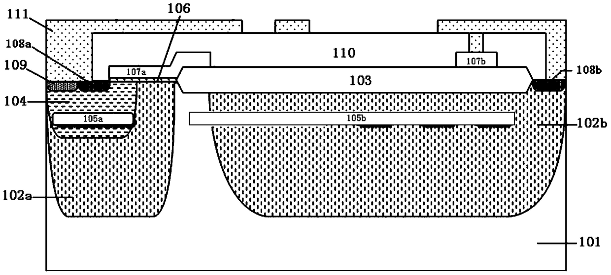
[0050] Isolated NLDMOS device, cell structure such as figure 2 As shown, two independent N-type deep wells, a left N-type deep well 102a and a right N-type deep well 102b, are formed on the P-type silicon substrate 101;

[0051] The left N-type deep well 102a has a P well 104 formed on the left;

[0052] In the P well 104, a P-type heavily doped region 109 and a source N-type heavily doped region 108a are formed on the left;

[0053]A gate oxide layer 106 is formed above the right part of the P well 104 and above the right part of the left N-type deep well 102a;

[0054] Field oxygen 103 is formed above the P-type silicon substrate 101 between the left N-type deep well 102a and the right N-type deep well 102b, and above the left part of the right N-type deep well 102b;

[0055] The right N-type deep well 102b has a drain N-type heavily doped region 108b formed on the right;

[0056] A gate polysilicon 107a is formed above the left part of the field oxygen 103 and above the...

Embodiment 2

[0069] The manufacturing method of the isolated NLDMOS device of Embodiment 1 includes the following process steps:

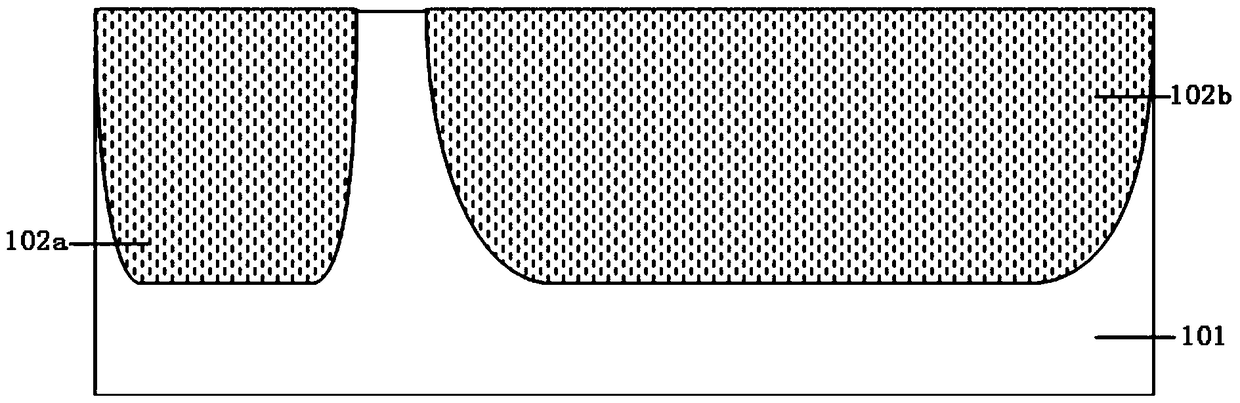
[0070] 1. On the P-type silicon substrate 101, two independent N-type deep wells, the left N-type deep well 102a and the right N-type deep well 102b, are formed by N-type ion implantation, as image 3 shown;

[0071] 2. Open the field oxygen region by using active region lithography, etch the field oxygen region above the P-type silicon substrate 101 between the left N-type deep well 102a and the right N-type deep well 102b, and the right N-type deep well 102b above the left part, growth field oxygen 103, such as Figure 4 shown;

[0072] 3. Photolithography opens the well implantation region, and implants P-type impurity ions into the left part of the left N-type deep well 102a to form a P well 104, such as Figure 5 As shown, the P well 104 serves as the background region of the isolated NLDMOS device;

[0073] Four. Carry out P-type ion implantation belo...


PUM


Abstract

The invention discloses an isolation N-type laterally diffused metal oxide semiconductor (NLDMOS) device. Two separate N-type deep well are formed on the P-type silicon substrate; left N-type deep well left portion is formed with a P-well; P-well left portion is formed with a P-type heavily doped region and an N-type heavily doped source miscellaneous areas; over the top and left-right portion of the N-type deep well P-well right portion formed with a gate oxide layer; N-type deep well with left and right P-type silicon N-type deep well between the top and right-left portion of the N-type deep well substrate above the field oxide is formed; the right N-type deep well right portion is formed with a drain terminal N-type heavily doped region; and a gate oxide layer over the top of the left part of the field oxide is formed with a gate polysilicon; P-type silicon substrate and the bottom of the field oxide Right N-type deep well formed in P-type implant drift region, the right of the P-type implant drift region as a staging interval shape. The invention also discloses a method for producing the isolated NLDMOS devices. The method can be isolated in ensuring NLDMOS device breakdown voltage does not decrease at the same time makes the device on-resistance is reduced.

Description

technical field [0001] The invention relates to semiconductor technology, in particular to an isolated NLDMOS device and a manufacturing method thereof. Background technique [0002] LDMOS (Laterally Diffused Metal Oxide Semiconductor) is currently widely used in power management circuits due to its advantages of high voltage resistance, high current drive capability, extremely low power consumption, and integration with CMOS. [0003] The isolated NLDMOS device not only has the high-voltage and high-current characteristics of discrete devices, but also absorbs the advantages of high-density intelligent logic control of low-voltage integrated circuits. A single chip realizes the functions that can only be completed by multiple chips, which greatly reduces the area, reduces costs, and improves It meets the development direction of miniaturization, intelligence and low energy consumption of modern power electronic devices. Breakdown voltage and on-resistance are key parameter...

Claims


Application Information

Patent Timeline
Patent Type & Authority Patents(China)
IPC IPC(8): H01L29/78H01L29/06H01L21/336
CPCH01L29/0607H01L29/66681H01L29/7816
Inventor 段文婷钱文生刘冬华
Owner SHANGHAI HUAHONG GRACE SEMICON MFG CORP
Why Eureka
Try Eureka