Trench MOSFET (Metal Oxide Semiconductor Field Effect Transistor) device and manufacturing method thereof

A manufacturing method and groove technology, which are applied in the manufacture of semiconductor/solid-state devices, semiconductor devices, electrical components, etc., can solve the problem of low withstand voltage in the terminal area, and achieve the effect of improving the withstand voltage and improving the withstand voltage

Active Publication Date: 2015-05-20
WUXI TONGFANG MICROELECTRONICS
View PDF6 Cites 7 Cited by
  • Summary
  • Abstract
  • Description
  • Claims
  • Application Information

AI Technical Summary

Problems solved by technology

[0007] In view of the above-mentioned shortcomings of the prior art, the purpose of the present invention is to provide a trench MOSFET device and its manufacturing method, which is used to solve the problem of low withstand voltage capability of the terminal region of the trench MOSFET device in the prior art

Method used


Image

  • Trench MOSFET (Metal Oxide Semiconductor Field Effect Transistor) device and manufacturing method thereof
  • Trench MOSFET (Metal Oxide Semiconductor Field Effect Transistor) device and manufacturing method thereof
  • Trench MOSFET (Metal Oxide Semiconductor Field Effect Transistor) device and manufacturing method thereof

Examples


Embodiment 1

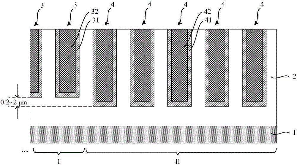
[0072] The present invention provides a trench MOSFET device, please refer to figure 1 , showing a cross-sectional view of the structure of the device, including an N-type heavily doped substrate 1 and an N-type lightly doped epitaxial layer 2 formed on the N-type heavily doped substrate 1; the N-type lightly doped epitaxial layer 2 A plurality of trench structures 3 in the cell region and a plurality of trench structures 4 in the termination region are formed in the layer 2 , wherein the depth of the trench structures 4 in the termination region is greater than the depth of the trench structures 3 in the cell region.

[0073] The cell region trench structure 3 is located in the cell region I of the trench MOSFET device, and the termination region trench structure 4 is located in the termination region II of the trench MOSFET device.

[0074] Specifically, the N-type heavily doped substrate 1 serves as the drain region of the trench MOSFET device, and the N-type lightly doped ...

Embodiment 2

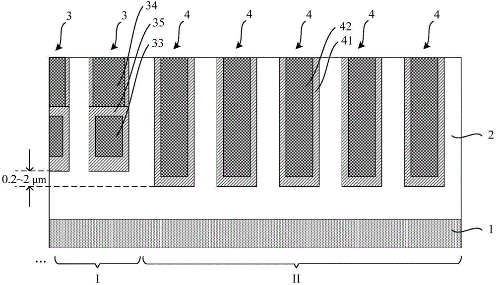
[0080] This embodiment adopts basically the same technical solution as Embodiment 1, the difference is that in Embodiment 1, the trench structure in the cell area adopts a conventional trench gate structure, while in this embodiment, the trench structure in the cell area The structure adopts the split gate structure.

[0081] see figure 2 , showing a cross-sectional view of the structure of a trench MOSFET device in this embodiment, including an N-type heavily doped substrate 1 and an N-type lightly doped epitaxial layer 2 formed on the N-type heavily doped substrate 1; In the N-type lightly doped epitaxial layer 2 are formed a plurality of trench structures 3 in the cell region and a plurality of trench structures 4 in the termination region, wherein: the trench structures 4 in the termination region are deeper than the trench structures 3 in the cell region depth.

[0082] Such as figure 2 As shown, the cell region trench structure 3 is a split gate, including a shieldi...

Embodiment 3

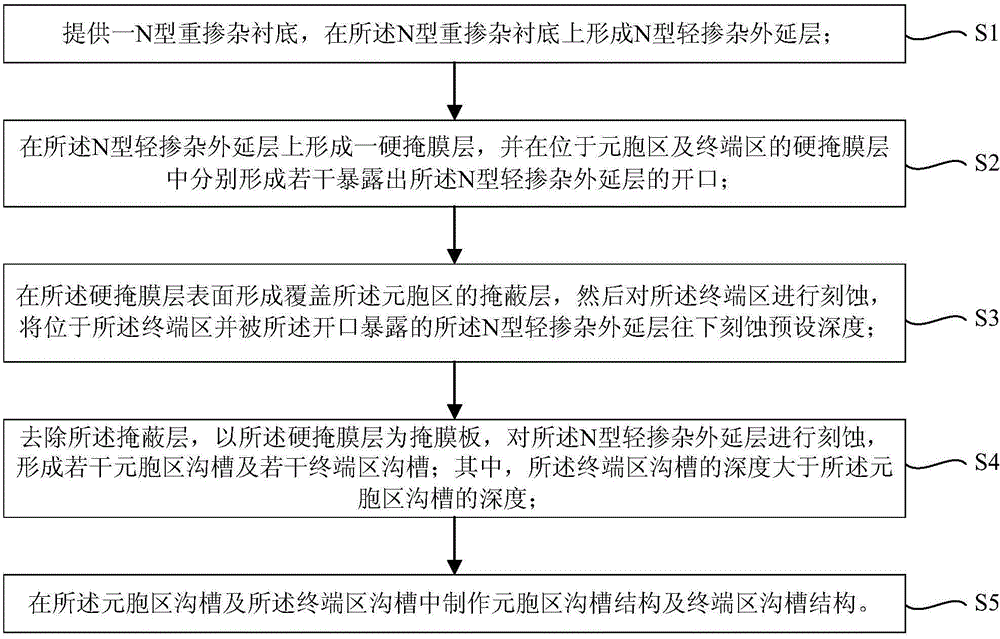
[0086] A kind of fabrication method of trench MOSFET device of the present invention is as follows, please refer to image 3 , shown as a process flow diagram of the method, at least comprising the following steps:

[0087] Step S1: providing an N-type heavily doped substrate, and forming an N-type lightly doped epitaxial layer on the N-type heavily doped substrate;

[0088] Step S2: forming a hard mask layer on the N-type lightly doped epitaxial layer, and forming a number of exposed N-type lightly doped epitaxial layers in the hard mask layer located in the cell region and the terminal region respectively. opening;

[0089] Step S3: Form a masking layer covering the cell region on the surface of the hard mask layer, and then etch the terminal region, and the N-type light located in the terminal region and exposed by the opening The doped epitaxial layer is etched down to a preset depth;

[0090] Step S4: removing the masking layer, using the hard mask layer as a mask, etc...


PUM


Abstract

The invention provides a trench MOSFET (Metal Oxide Semiconductor Field Effect Transistor) device and a manufacturing method thereof. The device comprises an N-type heavily doped substrate and an N-type lightly doped epitaxial layer which is formed on the N-type heavily doped substrate, wherein a plurality of cellular area trench structures and a plurality of terminal area trench structures are formed in the N-type lightly doped epitaxial layer; the depth of the terminal area trench structures is greater than the depth of the cellular area trench structures. Since an inversion layer is formed on the surface of a trench gate when the device is in work, the length of the inversion layer can be lengthened by the deeper terminal area trench structures, the depletion degree around the terminal area trench structures is higher; thus the voltage endurance capability of a medium pressure MOSFET terminal area is favorably improved.

Description

technical field [0001] The invention belongs to the field of electronic devices, and relates to a trench MOSFET device and a manufacturing method thereof. Background technique [0002] For semiconductor devices commonly used in power electronic systems and power management, the power Metal-Oxide-Semiconductor-Field-Effect-Transistor MOSFET (Metal-Oxide-Semiconductor-Field-Effect-Transistor), or Insulated Gate Field-Effect Transistor, is widely introduced . [0003] Trench power MOSFET is a new high-efficiency and power switching device developed after MOSFET. It adopts trench gate structure field effect transistor, which not only inherits the high input impedance of MOS field effect transistor (≥10 8 Ω), small driving current (about 0.1μA), and also has excellent characteristics such as high withstand voltage, large working current, high output power, good transconductance, and fast switching speed. It is precisely because it combines the advantages of electron tubes and p...

Claims


Application Information

Patent Timeline
Patent Type & Authority Applications(China)
IPC IPC(8): H01L29/78H01L29/06H01L21/336
CPCH01L29/06H01L29/4236H01L29/66477H01L29/78
Inventor 白玉明刘锋张海涛
Owner WUXI TONGFANG MICROELECTRONICS
Why Eureka
Try Eureka