Compound film solar battery and manufacturing method thereof

A technology of solar cells and compounds, applied in circuits, electrical components, photovoltaic power generation, etc., can solve the problems of low element content, toxic production process for human body, complexity, etc., and achieve the effect of low-cost production and excellent photovoltaic performance

Active Publication Date: 2015-05-27
HUAZHONG UNIV OF SCI & TECH
View PDF2 Cites 21 Cited by
  • Summary
  • Abstract
  • Description
  • Claims
  • Application Information

AI Technical Summary

Problems solved by technology

[0003] The invention provides a compound thin-film solar cell and a preparation method thereof, which solves the problems that the elements contained in the required mater

Method used


Image

  • Compound film solar battery and manufacturing method thereof
  • Compound film solar battery and manufacturing method thereof
  • Compound film solar battery and manufacturing method thereof

Examples


Embodiment 1

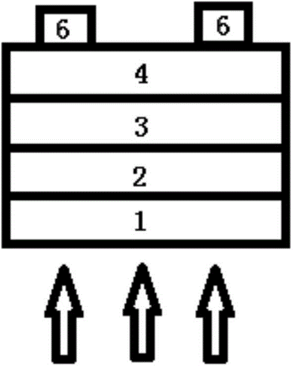
[0054] Embodiment 1, including the step of depositing a transparent electrode layer, the step of depositing an N-type buffer layer, the step of depositing a P-type absorber layer, and the step of depositing a back electrode layer:

[0055] 1. The step of depositing a transparent electrode layer: depositing a transparent electrode layer 2 on the surface of the substrate 1 by magnetron sputtering;

[0056] The substrate is glass with a thickness of 3.2cm;

[0057] The transparent electrode layer is SnO 2 : F, the thickness is 800nm;

[0058] 2. The step of depositing an N-type buffer layer: depositing an N-type buffer layer 3 on the transparent electrode layer 2 by a solution coating method;

[0059] The N-type buffer layer is TiO 2 Material, with a thickness of 500nm;

[0060] Add 50ml of absolute ethanol, 7.5ml of triethanolamine, and 8.5ml of tetra-n-butyl titanate to the flask in turn, seal the flask and stir for 2 hours, then add 10ml of glacial acetic acid and 10ml of ...

Embodiment 2

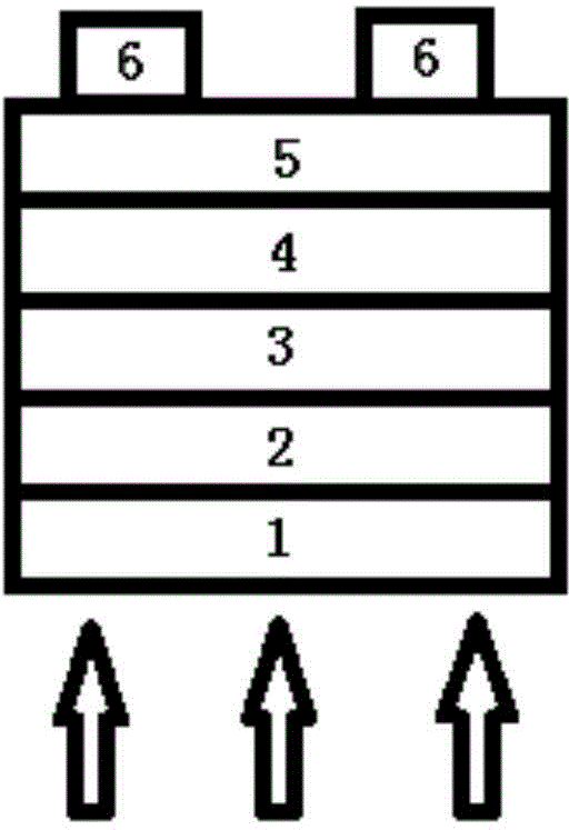
[0067] Embodiment 2, including the step of depositing a transparent electrode layer, the step of depositing an N-type buffer layer, the step of depositing a P-type absorber layer, and the step of depositing a back electrode layer:

[0068] 1. The step of depositing a transparent electrode layer: depositing a transparent electrode layer 2 on the surface of the substrate 1 by electron beam evaporation;

[0069] The substrate is glass with a thickness of 3.2cm;

[0070] The transparent electrode layer is SnO 2 : F, the thickness is 1000nm;

[0071] 2. The step of depositing an N-type buffer layer: depositing an N-type buffer layer 3 on the transparent electrode layer 2 by a solution coating method;

[0072] The N-type buffer layer is a ZnO material with a thickness of 500nm;

[0073] 1.1g of Zn(Ac)2·2H2O and 0.29g of LiOH·H2O were respectively dissolved in 50mL of absolute ethanol, cooled to 0°C, titrated the LiOH solution into Zn(Ac)2 in 10 minutes, and stirred for 1 hour Ta...

Embodiment 3

[0079] Embodiment 3, including the step of depositing a transparent electrode layer, the step of depositing an N-type buffer layer, the step of depositing a P-type absorber layer, and the step of depositing a back electrode layer:

[0080] 1. The step of depositing a transparent electrode layer: depositing a transparent electrode layer 2 on the surface of the substrate 1 by magnetron sputtering;

[0081] The substrate is glass with a thickness of 3.2cm;

[0082] The transparent electrode layer is SnO 2 : F, the thickness is 800nm;

[0083] 2. The step of depositing an N-type buffer layer: depositing an N-type buffer layer 3 on the transparent electrode layer 2 by electron beam evaporation;

[0084] The N-type buffer layer is TiO 2 material, the thickness is 120nm;

[0085] Using TiO 2 target, pump the chamber to a vacuum of 5×10 -4 Pa, rotate the substrate table at a speed of 3rpm, wait until the substrate temperature is heated to 350°C, and pre-melt the TiO with the ele...


PUM

PropertyMeasurementUnit
Thicknessaaaaaaaaaa
Thicknessaaaaaaaaaa
Thicknessaaaaaaaaaa

Abstract

The invention discloses a compound film solar battery and a manufacturing method thereof, belongs to the field of preparation of semiconductor photoelectric materials and film solar batteries, and solves the problems that materials for a compound film solar battery are relatively small in content in the earthcrust, high in price and toxic for human bodies. The compound film solar battery comprises a substrate, a transparent electrode layer, an N-type buffer layer, a P-type absorbing layer and a back electrode layer, wherein the P-type absorbing layer is made of materials such as Sb2Se3, Cu3SbS3 and Cu3SbS4. The manufacturing method comprises steps of depositing the transparent electrode layer, depositing the N-type buffer layer, depositing the P-type buffer layer and depositing the electrode layer, and a step of depositing a hole conduction layer can also be added. Various materials forming the P-type absorbing layer are all selected from elements which are rich in resource and free of toxic component, the environment is not polluted when the compound film solar battery is manufactured and used, the energy gap width of the material of the P-type absorbing layer ranges from about 0.5 ev to 2.5 ev, the spectral response range is relatively wide, and the light absorption coefficient is as high as 10<5> cm<-1>.

Description

technical field [0001] The invention belongs to the field of semiconductor photoelectric materials and thin-film solar cell preparation, and in particular relates to an antimony-based compound thin-film solar cell and a preparation method thereof. Background technique [0002] With the advent of the global energy crisis and the increasingly serious environmental pollution problem, the research on clean and pollution-free energy is imminent. As a clean and abundant energy source, solar energy has attracted widespread attention. How to prepare solar cells with lower cost and higher conversion efficiency is the focus of research. A solar cell is a device that uses the photovoltaic effect to directly convert solar energy into electrical energy. Multi-component compound thin-film solar cells have received more attention due to their advantages such as less material consumption, low energy consumption for preparation, good low-light and high-temperature performance, light weight...

Claims


Application Information

Patent Timeline
IPC IPC(8): H01L31/032H01L31/072H01L31/18
CPCY02E10/50Y02P70/50
Inventor 唐江周英冷美英刘新胜韩珺罗苗
Owner HUAZHONG UNIV OF SCI & TECH
Why Eureka
Try Eureka