Production method of twin-structure hard alloy matrix
A technology of cemented carbide substrate and production method, applied in the field of cemented carbide substrate, can solve the problems of inapplicability, large proportion of fine tungsten carbide, high hardness and the like
- Summary
- Abstract
- Description
- Claims
- Application Information
AI Technical Summary
Problems solved by technology
Method used
Image
Examples
Embodiment 1
[0027] A production method of a twin crystal structure cemented carbide substrate, which comprises the steps of:
[0028] 1, batching: prepare compound according to the component of embodiment 1 in table 1;
[0029] 2. Ball milling: mill the above mixture in a ball mill; the milling time is 48 hours.
[0030] 3. Granulating, granulating the mixture after ball milling;
[0031] 4. Compression molding, pressing the mixture into alloy semi-finished products in the desired shape;
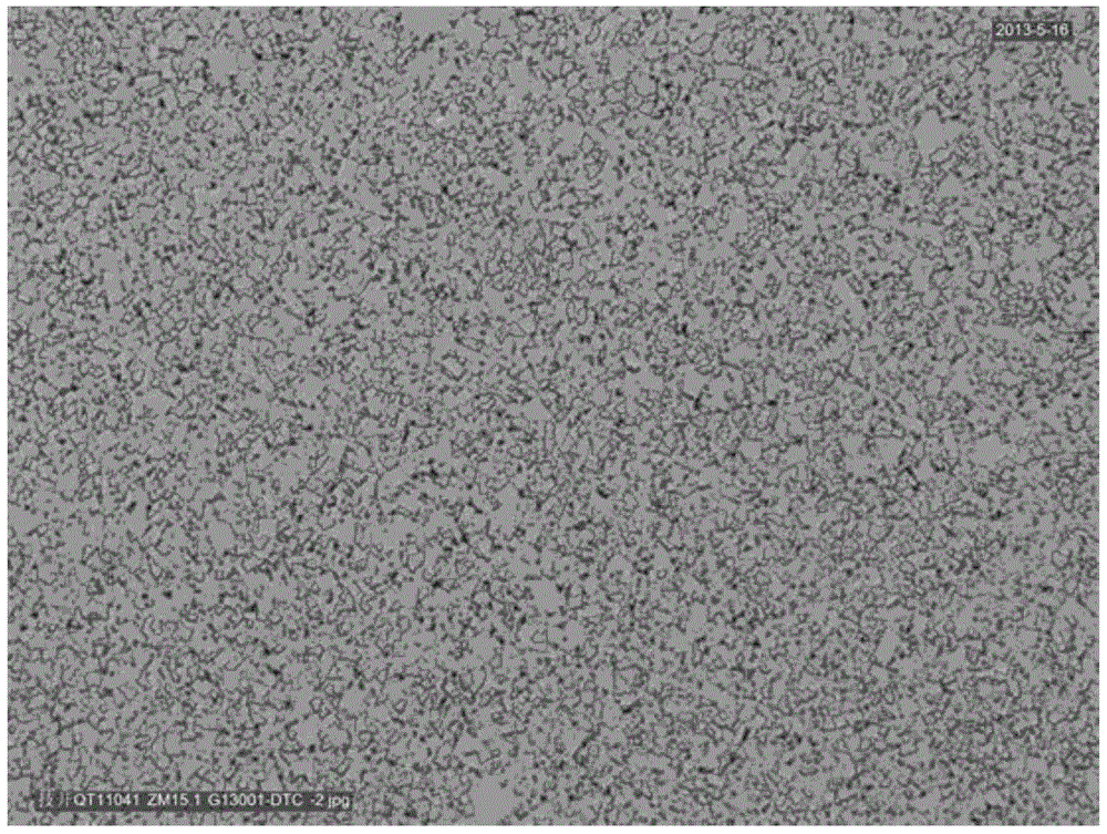
[0032] 5. Sintering, put the semi-finished product in a sintering furnace and sinter it with hydrogen dewaxing and positive pressure at 1460-1480°C; obtain a cemented carbide matrix. The metallographic photo of the cemented carbide substrate magnified 1500 times is as follows figure 1 .
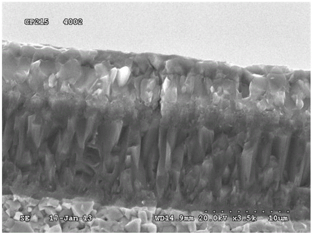
[0033] 6. The cemented carbide substrate is subjected to CVD coating after surface treatment. SEM photographs of coated alloys as figure 2 shown. Coatings include:
[0034] The first layer (adjacent to the cem...
Embodiment 2
[0042] The production method of the twin crystal structure cemented carbide substrate of the present invention, except following steps, other is with embodiment 1:
[0043] 1, batching: prepare compound according to the component of embodiment 2 in table 1;
[0044] 6. The cemented carbide substrate is subjected to CVD coating after surface treatment. Coatings include:
[0045] The first layer (adjacent to the cemented carbide substrate) is a TiN layer with a thickness of 0.1-1 μm, equiaxed grains, and an average grain size ≤ 0.5 μm;
[0046] The second layer is a Ti(C,N) layer deposited by medium-temperature CVD, with a thickness of 6-9 μm, columnar crystals, and an average grain size of 0.5-2 μm;
[0047] The third layer is a TiCNO transition layer with a thickness of 0.1-1 μm, equiaxed grains, and an average grain size of ≤0.5 μm;
[0048] The fourth layer is ɑ-Al 2 o 3 layer, thickness 4-5.5 μm, equiaxed grains, average grain size 0.5-2 μm;
[0049] The fifth layer i...
Embodiment 3
[0055] The production method of the twin crystal structure cemented carbide substrate of the present invention, except following steps, other is with embodiment 1:
[0056] 1, batching: prepare compound according to the component of embodiment 3 in table 1;
[0057] 6. The cemented carbide substrate is subjected to CVD coating after surface treatment. Coatings include:
[0058] The first layer (adjacent to the cemented carbide substrate) is a TiN layer with a thickness of 0.1-1 μm, equiaxed grains, and an average grain size ≤ 0.5 μm;
[0059] The second layer is a Ti(C,N) layer deposited by medium-temperature CVD, with a thickness of 8-12 μm, columnar crystals, and an average grain size of 0.5-2 μm;
[0060] The third layer is a TiCNO transition layer with a thickness of 0.1-1 μm, equiaxed grains, and an average grain size of ≤0.5 μm;
[0061] The fourth layer is ɑ-Al 2 o 3 Layer, thickness 4-7μm, equiaxed grains, average grain size 0.5-2μm;
[0062] The fifth layer is a T...
PUM
| Property | Measurement | Unit |
|---|---|---|
| Thickness | aaaaa | aaaaa |
| Average grain size | aaaaa | aaaaa |
| Thickness | aaaaa | aaaaa |
Abstract
Description
Claims
Application Information


