Graphene field effect transistor terahertz wave modulator and manufacture method thereof

A field effect transistor, terahertz wave technology, applied in the terahertz wave application field, can solve the problems of multiple defects, multiple pinholes, and low breakdown voltage, so as to improve the modulation rate and relative modulation depth, reduce leakage current, The effect of reducing thickness

Inactive Publication Date: 2015-06-03
UNIV OF ELECTRONICS SCI & TECH OF CHINA
View PDF3 Cites 26 Cited by
  • Summary
  • Abstract
  • Description
  • Claims
  • Application Information

AI Technical Summary

Problems solved by technology

[0003] In recent years, traditional graphene field effect transistor terahertz wave modulators use SiO with a thickness of 300nm or 98nm. 2 As a dielectric layer, but due to the thermal evaporation growth process is easy to cause SiO 2 Uneven surface, multiple defects, and multiple pinholes lead to large leakage current of the transistor and relatively low breakdown voltage, and the modulation rate and modulation depth of the terahertz wave modulator need to be improved

Method used


Image

  • Graphene field effect transistor terahertz wave modulator and manufacture method thereof
  • Graphene field effect transistor terahertz wave modulator and manufacture method thereof
  • Graphene field effect transistor terahertz wave modulator and manufacture method thereof

Examples


Embodiment Construction

[0029] The present invention will be described in further detail below in conjunction with specific embodiments and accompanying drawings. It should be noted that the present invention is not limited to the embodiments.

[0030] The preparation of graphene field effect transistor terahertz wave modulator comprises the following steps:

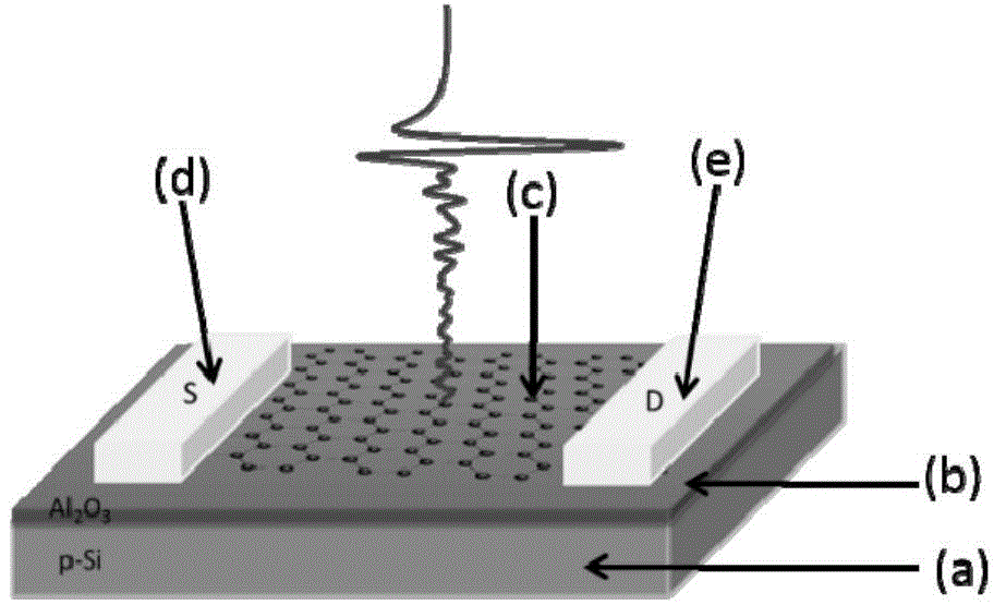
[0031] Step 1. Cleaning the semiconductor substrate (a): first put the Si substrate into a beaker filled with acetone and perform ultrasonic cleaning for 10 minutes, then put the Si substrate into a beaker filled with alcohol for ultrasonic cleaning for 10 minutes, and finally use Rinse with deionized water, put the cleaned Si substrate into an oven and dry at 120°C for 2 hours for later use;

[0032] Step 2. Deposit dielectric layer: Deposit Al on the front side of the Si substrate by atomic layer deposition (ALD) 2 o 3For the dielectric layer, trimethylaluminum (TMA) is used as the aluminum source, oxygen is used as the reaction gas, and ar...


PUM

PropertyMeasurementUnit
thicknessaaaaaaaaaa
sizeaaaaaaaaaa
sizeaaaaaaaaaa

Abstract

The invention provides a graphene field effect transistor terahertz wave modulator and a manufacture method thereof and aims to increase the modulating speed and depth of the graphene field effect transistor terahertz wave modulator. The graphene field effect transistor terahertz wave modulator comprises a semiconductor substrate, and a medium layer, a graphene film and source and drain electrodes which are arranged on the substrate, and an annular grating electrode which is arranged on the back of the substrate. The terahertz wave modulator is characterized in that the medium layer is an Al2O3 layer, and the thickness ranges from 5 to 100nm; the Al2O3 is deposited by the ALD (atomic layer deposition) method, and the Al2O3 is high in evenness, is free of defects and pores and has better voltage resistance; the leakage current is reduced greatly. The modulating speed of the terahertz wave modulator can be 178 KHz, the corresponded modulating depth is larger than 22%, and the modulating speed and depth are increased significantly; the terahertz wave modulator can be widely applied to the fields of terahertz wave communication systems, terahertz wave detection and terahertz wave imaging.

Description

technical field [0001] The invention belongs to the technical field of terahertz wave application, and designs a terahertz wave modulator and a preparation method thereof, in particular to a graphene field effect transistor terahertz wave modulator and a preparation method thereof. Background technique [0002] Terahertz wave (THz) usually refers to electromagnetic radiation with a frequency in the range of 0.1THz-10THz (1THz=1012Hz), which is in the transition region between macroelectronics and microphotonics. Terahertz waves are the focus of next-generation communication technology. They are ideal tools for biomedical research and biochemical weapon detection. They also have very important applications in nondestructive testing, security inspections, and radar imaging. Graphene, as a two-dimensional monoatomic layer film material of carbon allotrope, has been discovered since 2004 with its unique structure, extraordinary electrical properties, optical properties, good mec...

Claims


Application Information

Patent Timeline
Patent Type & Authority Applications(China)
IPC IPC(8): G02F1/015
CPCG02F1/015
Inventor 文岐业毛淇田伟陈智杨青慧张怀武沈雁飞
Owner UNIV OF ELECTRONICS SCI & TECH OF CHINA
Why Eureka
Try Eureka