Dual trapped wave flat ultra wideband antenna

A technology of ultra-wideband antenna and double-notch wave, which is applied in the field of double-notch planar ultra-wideband antenna, can solve problems such as mismatching between antenna and microwave circuit, endangering the normal operation of the system, complex antenna structure and process, etc., and achieve good omnidirectional Radiation characteristics, design cost reduction, effects of good notch characteristics

Inactive Publication Date: 2015-06-03
HARBIN HESON SCI & TECH
View PDF0 Cites 13 Cited by
  • Summary
  • Abstract
  • Description
  • Claims
  • Application Information

AI Technical Summary

Problems solved by technology

[0003] However, the frequency band occupied by the current ultra-wideband communication shares some with WiMAX and wireless local area network, so it is necessary to design an antenna that can reduce the interference to it. Designing an ultra-wideband antenna with notch characteristics has become a current research hotspot.
If there is no proper design to suppress harmonic resonance and spurious emission, the antenna will cause electromagnetic interference to nearby equipment, endangering the normal operation of the system itself and adjacent systems, especially causing interference to the currently used LAN system
Adding a filter is the most commonly used method to solve this kind of problem, but it often causes a mismatch between the antenna and the microwave circuit, and even reduces the overall performance of the system. Therefore, designing an ultra-wideband antenna with notch characteristics is the best way to solve this problem. One of the important methods, while solving the current complex problems of the structure and technology of the antenna

Method used


Image

  • Dual trapped wave flat ultra wideband antenna
  • Dual trapped wave flat ultra wideband antenna
  • Dual trapped wave flat ultra wideband antenna

Examples


Embodiment 1

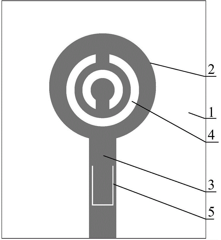
[0022] Such as figure 1 As shown, the dual-notch planar UWB antenna consists of: a dielectric substrate (1), a radiating element (2), a signal feeding strip line (3), and a circular complementary split resonant ring (CSRR) on the radiating element structure (4), open a U-shaped slot (5) on the signal feeder strip line. The radiating unit and the signal feeder strip line are printed on the upper surface of the dielectric substrate, the radiating unit is located in the middle of the dielectric substrate, the feeder leads from the edge of the dielectric substrate to the radiating unit and is connected to it, and the ground plane is printed on the dielectric substrate. the lower surface of the substrate.

[0023] The dielectric substrate is made of polytetrafluoroethylene with a thickness of 1.6 mm and a relative dielectric constant of 4.4.

[0024] The characteristic impedance of the coplanar waveguide feeding stripline is 50Ω, and the line width is 3.3mm.
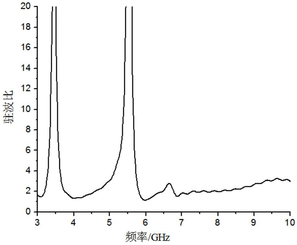
[0025] figure 2 ...


PUM


Abstract

The invention discloses a dual trapped wave flat ultra wideband antenna which consists of a medium substrate (1), a radiation unit (2) and a signal feed band wire (3), wherein a circular complementation opening resonance ring (CSRR) structure (4) is arranged on the radiation unit; the signal feed band wire is provided with a U-shaped slot (5); the radiation unit and the signal feed band wire are both printed at the upper surface of the medium substrate; the radiation unit is positioned in the middle of the medium substrate; a feeder is led to the radiation unit from the margin of the medium substrate and connected with the same, and a grounding surface is printed at the lower surface of the medium substrate. The dual trapped wave flat ultra wideband antenna is compact in structure and small in size; trapped wave frequency can be regulated by changing the size and position of the U-shaped slot and the circular complementation opening resonance ring (CSRR) structure, and the problem of same frequency interference of an ultra wideband communication system is solved.

Description

technical field [0001] The invention designs an antenna, in particular to a double-notch planar ultra-wideband antenna. Background technique [0002] Since the US Federal Communications Commission (Federal Communications Commission) allowed the commercial use of the 3.1-10.6GHz frequency band, ultra-wideband technology has received wider attention in the academic and commercial fields. The coplanar waveguide structure that does not require drilling and is easy to integrate is changing day by day, and the structure can be fabricated by photographic technology and has good polarization characteristics, so this technology has been applied to the design of ultra-wideband antennas and related microwave circuit components in the design. [0003] However, the frequency band occupied by the current ultra-wideband communication shares with WiMAX and wireless local area network, so it is necessary to design an antenna that can reduce the interference to it. Designing an ultra-wideban...

Claims


Application Information

Patent Timeline
Patent Type & Authority Applications(China)
IPC IPC(8): H01Q1/36H01Q1/48
Inventor 李琦张道亮金佳佳
Owner HARBIN HESON SCI & TECH
Why Eureka
Try Eureka